- 您現(xiàn)在的位置:買(mǎi)賣IC網(wǎng) > PDF目錄383640 > MT3170BE (Mitel Networks Corporation) Wide Dynamic Range DTMF Receiver PDF資料下載
參數(shù)資料
| 型號(hào): | MT3170BE |
| 廠商: | Mitel Networks Corporation |
| 英文描述: | Wide Dynamic Range DTMF Receiver |
| 中文描述: | 寬動(dòng)態(tài)范圍的DTMF接收器 |
| 文件頁(yè)數(shù): | 2/8頁(yè) |
| 文件大小: | 91K |
| 代理商: | MT3170BE |
MT3170B/71B, MT3270B/71B, MT3370B/71B
4-4
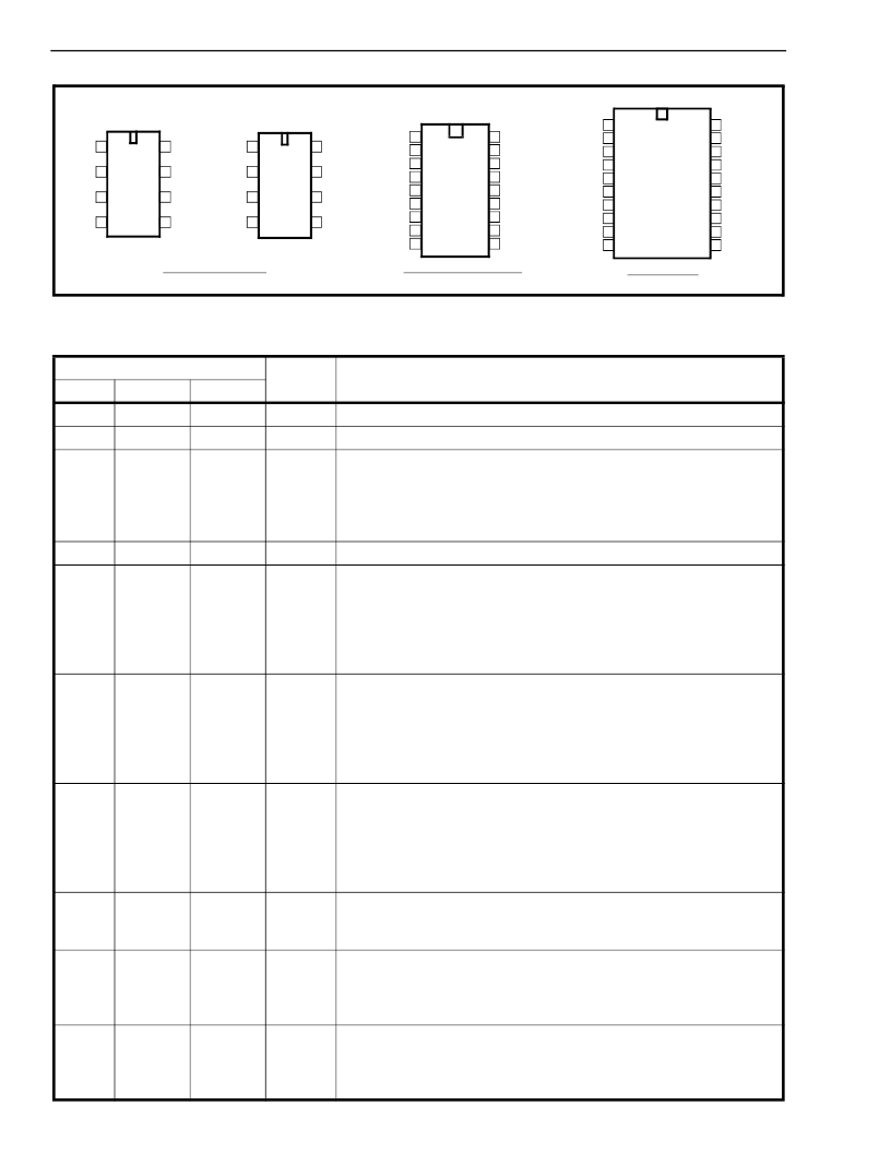
Figure 2 - Pin Connections
Pin Description
Pin #
327xB
1
2
3
Name
Description
337xB
2
4
6
317xB
1
-
3
INPUT
OSC2
OSC1
(CLK)
DTMF/CP Input.
Input signal must be AC coupled via capacitor.
Oscillator Output.
Oscillator/Clock Input.
This pin can either be driven by:
1)
an external digital clock with defined input logic levels. OSC2
should be left open.
2)
connecting a crystal or ceramic resonator between OSC1 and
OSC2 pins.
Ground.
(0V)
Serial Data/Call Progress Output.
This pin serves the dual function
of being the serial data output when clock pulses are applied after
validation of DTMF signal, and also indicates the cadence of call
progress input. As DTMF signal lies in the same frequency band as
call progress signal, this pin may toggle for DTMF input. The SD pin
is at logic low in powerdown state.
Acknowledge Pulse Input.
After ESt or DStD is high, applying a
sequence of four pulses on this pin will then shift out four bits on the
SD pin, representing the decoded DTMF digit. The rising edge of the
first clock is used to latch the 4-bit data prior to shifting. This pin is
pulled down internally. The idle state of the ACK signal should be
low.
Early Steering Output.
A logic high on ESt indicates that a DTMF
signal is present. ESt is at logic low in powerdown state.
9
11
4
5
4
5
V
SS
SD
13
6
6
ACK
15
7
7
ESt
(MT3x70B)
DStD
(MT3x71B)
Delayed Steering Output.
A logic high on DStD indicates that a
valid DTMF digit has been detected. DStD is at logic low in
powerdown state.
Positive Power Supply (5V Typ.)
Performance of the device can be
optimized by minimizing noise on the supply rails. Decoupling
capacitors across V
DD
and V
SS
are therefore recommended.
No Connection.
Pin is unconnected internally.
18
8
8
V
DD
1,5,7,8,
10, 12,
14,16,
17
3
-
-
NC
-
2
PWDN
Power Down Input.
A logic high on this pin will power down the
device to reduce power consumption. This pin is pulled down
internally and can be left open if not used. ACK pin should be at logic
’0’ to power down device.
10
18
17
16
15
14
13
12
11
VDD
NC
NC
ESt/DStD
NC
ACK
NC
SD
NC
1
2
3
4
5
6
7
8
9
NC
INPUT
PWDN
OSC2
NC
OSC1
NC
NC
VSS
INPUT
PWDN
CLK
VSS
VDD
ESt/
DStD
ACK
SD
INPUT
OSC2
OSC1
VSS
VDD
ESt/
DStD
ACK
SD
MT3170B/71B
MT3270B/71B
MT3370B/71B
8 PIN PLASTIC DIP
18 PIN PLASTIC SOIC
1
2
3
4
8
7
6
5
1
2
3
4
8
7
6
5
1
2
3
4
5
6
7
8
9
10
11
12
20
19
18
17
16
15
14
13
NC
NC
INPUT
PWDN
NC
NC
NC
OSC1
VSS
OSC2
20 PIN SSOP
NC
VDD
NC
ESt/DStD
NC
ACK
SD
NC
NC
MT3370B/71B
NC
相關(guān)PDF資料 |
PDF描述 |
|---|---|
| MT3170 | Wide Dynamic Range DTMF Receiver |
| MT3170B | Wide Dynamic Range DTMF Receiver |
| MT3270 | Wide Dynamic Range DTMF Receiver |
| MT3170B | Wide Dynamic Range DTMF Receiver(50dB的寬動(dòng)態(tài)范圍雙音多頻信號(hào)(DTMF)接收器) |
| MT3171B | Wide Dynamic Range DTMF Receiver(50dB的寬動(dòng)態(tài)范圍雙音多頻信號(hào)(DTMF)接收器) |
相關(guān)代理商/技術(shù)參數(shù) |
參數(shù)描述 |
|---|---|
| MT3170BE1 | 制造商:Microsemi Corporation 功能描述:DTMF RX 4.19MHZ 5V 8PDIP - Rail/Tube |
| MT3171B | 制造商:ZARLINK 制造商全稱:Zarlink Semiconductor Inc 功能描述:Wide Dynamic Range DTMF Receiver |
| MT3171BE | 制造商:Microsemi Corporation 功能描述: |
| MT3171BE1 | 制造商:Microsemi Corporation 功能描述:DTMF RX 4.19MHZ 5V 8PDIP - Rail/Tube 制造商:MICROSEMI CONSUMER MEDICAL PRODUCT GROUP 功能描述:IC RECEIVER DTMF 50DB 8PDIP 制造商:Microsemi Corporation 功能描述:IC RECEIVER DTMF 50DB 8PDIP |
| MT3173-Y | 制造商:MARKTECH 制造商全稱:Marktech Corporate 功能描述:Reflector Cap Rectangular LED Lamps |
發(fā)布緊急采購(gòu),3分鐘左右您將得到回復(fù)。