- 您現(xiàn)在的位置:買賣IC網(wǎng) > PDF目錄382347 > MR82510 (Intel Corp.) ASYNCHRONOUS SERIAL CONTROLLER PDF資料下載
參數(shù)資料
| 型號: | MR82510 |
| 廠商: | Intel Corp. |
| 英文描述: | ASYNCHRONOUS SERIAL CONTROLLER |
| 中文描述: | 異步串行控制器 |
| 文件頁數(shù): | 4/40頁 |
| 文件大?。?/td> | 463K |
| 代理商: | MR82510 |
第1頁第2頁第3頁當前第4頁第5頁第6頁第7頁第8頁第9頁第10頁第11頁第12頁第13頁第14頁第15頁第16頁第17頁第18頁第19頁第20頁第21頁第22頁第23頁第24頁第25頁第26頁第27頁第28頁第29頁第30頁第31頁第32頁第33頁第34頁第35頁第36頁第37頁第38頁第39頁第40頁
M82510
GENERAL DESCRIPTION
The M82510 can be functionally divided into seven
major blocks (See Fig 1): Bus Interface Unit, Timing
Unit, Modem Module, Tx FIFO, Rx FIFO, Tx Ma-
chine, and Rx Machine. Six of these blocks (all ex-
cept Bus Interface Unit) can generate block inter-
rupts. Three of these blocks can generate second-
level interrupts which reflect errors/status within the
block (Receive Machine, Timing Unit, and the Mo-
dem Module).
The Bus interface unit allows the M82510 to inter-
face with the rest of the system. It controls access to
device registers as well as generation of interrupts
to the external world. The FIFOs buffer the CPU
from the Serial Machines and reduce the interrupt
overhead normally required for serial operations.
The threshold (level of occupancy in the FIFO which
will generate an interrupt) is programmable for each
FIFO. The timing unit controls generation of the sys-
tem clock through either its on-chip crystal oscillator,
or an externally generated clock. It also provides two
Baud Rate Generators/Timers with various options
and modes to support serial communication.
FUNCTIONAL DESCRIPTION
CPU Interface
The M82510 has a simple demultiplexed Bus Inter-
face, which consists of a bidirectional three-state
eight-bit, data bus and a three-bit address bus. An
Interrupt pin along with the Read, Write and Chip
Select are the remaining signals used to interface
with the CPU. The three address lines along with the
Bank Pointer register are used to select the regis-
ters. The M82510 is designed to interface to all Intel
microprocessor and microcontroller families. Like
most other I/O based peripherals it is programmed
through its registers to support a variety of functions.
Its register set can be used in 8250A/16450 com-
patibility or High Performance modes. The 8250A/
16450 mode is the default wake-up mode in which
only the 8250A/16450 compatible registers are ac-
cessible. The remaining registers are default config-
ured to support 8250A/16450 emulation.
Software Interface
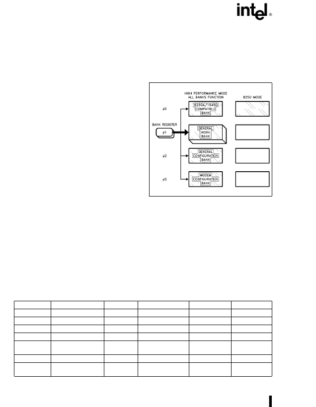
271072–3
Figure 3. M82510 Register Architecture
The M82510 is configured and controlled through its
35 registers which are divided into four banks. Only
one bank is accessible at any one time. The bank
switching is done by changing the contents of the
bank pointer (GIR/BANK–BANK0, BANK1). The
banks are logically grouped into 8250A/16450 com-
patible (0), General Work Bank (1), General Configu-
ration (2), and Modem Configuration (3). The
8250A/16450 compatible bank (Bank 0) is the de-
fault bank upon power up.
The M82510 registers can be categorized under the
following:
Table 2. M82510 Register/Block Functions
Status
Enable
Configuration
Command
Data
FIFO
FLR
D
FMD
D
D
MODEM
MSR
MIE
PMD
MCR
D
RX
RST, RXF
RIE
RMD
RCM
RXD, RXF
TX
LSR
LSR
TMD
TCM
TXD, TXF
TIMER
TMST
TMIE
CLCF,
TMCR
BBL, BBH
BAL, BAH
BACF, BBCF
DEVICE
GSR, GIR
GER
IMD
ICM
D
8250
LSR, MSR, GIR
GER
LCR, MCR
MCR
TXD, RXD
BAL, BAH
4
相關PDF資料 |
PDF描述 |
|---|---|
| MR8251A | PROGRAMMABLE COMMUNICATION INTERFACE |
| MR851G | Axial Lead Fast Recovery Rectifiers |
| MR851RL | Axial Lead Fast Recovery Rectifiers |
| MR851RLG | Axial Lead Fast Recovery Rectifiers |
| MR852G | Axial Lead Fast Recovery Rectifiers |
相關代理商/技術參數(shù) |
參數(shù)描述 |
|---|---|
| MR82510/B | 制造商:Rochester Electronics LLC 功能描述: |
| MR8251A | 制造商:Intel 功能描述: |
| MR8251A/B | 制造商:Rochester Electronics LLC 功能描述: |
| MR8254/B | 制造商:Rochester Electronics LLC 功能描述: |
| MR8254/R | 制造商:Rochester Electronics LLC 功能描述:- Bulk |
發(fā)布緊急采購,3分鐘左右您將得到回復。