- 您現(xiàn)在的位置:買賣IC網(wǎng) > PDF目錄45379 > MR80C32E-30SBD (ATMEL CORP) 8-BIT, 30 MHz, MICROCONTROLLER, CQCC44 PDF資料下載
參數(shù)資料
| 型號: | MR80C32E-30SBD |
| 廠商: | ATMEL CORP |
| 元件分類: | 微控制器/微處理器 |
| 英文描述: | 8-BIT, 30 MHz, MICROCONTROLLER, CQCC44 |
| 封裝: | LCC-44 |
| 文件頁數(shù): | 17/286頁 |
| 文件大小: | 9413K |
| 代理商: | MR80C32E-30SBD |
第1頁第2頁第3頁第4頁第5頁第6頁第7頁第8頁第9頁第10頁第11頁第12頁第13頁第14頁第15頁第16頁當前第17頁第18頁第19頁第20頁第21頁第22頁第23頁第24頁第25頁第26頁第27頁第28頁第29頁第30頁第31頁第32頁第33頁第34頁第35頁第36頁第37頁第38頁第39頁第40頁第41頁第42頁第43頁第44頁第45頁第46頁第47頁第48頁第49頁第50頁第51頁第52頁第53頁第54頁第55頁第56頁第57頁第58頁第59頁第60頁第61頁第62頁第63頁第64頁第65頁第66頁第67頁第68頁第69頁第70頁第71頁第72頁第73頁第74頁第75頁第76頁第77頁第78頁第79頁第80頁第81頁第82頁第83頁第84頁第85頁第86頁第87頁第88頁第89頁第90頁第91頁第92頁第93頁第94頁第95頁第96頁第97頁第98頁第99頁第100頁第101頁第102頁第103頁第104頁第105頁第106頁第107頁第108頁第109頁第110頁第111頁第112頁第113頁第114頁第115頁第116頁第117頁第118頁第119頁第120頁第121頁第122頁第123頁第124頁第125頁第126頁第127頁第128頁第129頁第130頁第131頁第132頁第133頁第134頁第135頁第136頁第137頁第138頁第139頁第140頁第141頁第142頁第143頁第144頁第145頁第146頁第147頁第148頁第149頁第150頁第151頁第152頁第153頁第154頁第155頁第156頁第157頁第158頁第159頁第160頁第161頁第162頁第163頁第164頁第165頁第166頁第167頁第168頁第169頁第170頁第171頁第172頁第173頁第174頁第175頁第176頁第177頁第178頁第179頁第180頁第181頁第182頁第183頁第184頁第185頁第186頁第187頁第188頁第189頁第190頁第191頁第192頁第193頁第194頁第195頁第196頁第197頁第198頁第199頁第200頁第201頁第202頁第203頁第204頁第205頁第206頁第207頁第208頁第209頁第210頁第211頁第212頁第213頁第214頁第215頁第216頁第217頁第218頁第219頁第220頁第221頁第222頁第223頁第224頁第225頁第226頁第227頁第228頁第229頁第230頁第231頁第232頁第233頁第234頁第235頁第236頁第237頁第238頁第239頁第240頁第241頁第242頁第243頁第244頁第245頁第246頁第247頁第248頁第249頁第250頁第251頁第252頁第253頁第254頁第255頁第256頁第257頁第258頁第259頁第260頁第261頁第262頁第263頁第264頁第265頁第266頁第267頁第268頁第269頁第270頁第271頁第272頁第273頁第274頁第275頁第276頁第277頁第278頁第279頁第280頁第281頁第282頁第283頁第284頁第285頁第286頁
113
8183F–AVR–06/12
ATtiny24A/44A/84A
13. Timer/Counter Prescaler
Timer/Counter0 and Timer/Counter1 share the same prescaler module, but the Timer/Counters
can have different prescaler settings. The description below applies to both Timer/Counters. Tn
is used as a general name, n = 0, 1.
The Timer/Counter can be clocked directly by the system clock (by setting the CSn[2:0] = 1).
This provides the fastest operation, with a maximum Timer/Counter clock frequency equal to
system clock frequency (f
CLK_I/O). Alternatively, one of four taps from the prescaler can be used
as a clock source. The prescaled clock has a frequency of either f
CLK_I/O/8, fCLK_I/O/64,
f
CLK_I/O/256, or fCLK_I/O/1024.
13.1
Prescaler Reset
The prescaler is free running, i.e., operates independently of the Clock Select logic of the
Timer/CounterCounter, and it is shared by the Timer/Counter Tn. Since the prescaler is not
affected by the Timer/Counter’s clock select, the state of the prescaler will have implications for
situations where a prescaled clock is used. One example of prescaling artifacts occurs when the
timer is enabled and clocked by the prescaler (CSn[2:0] = 2, 3, 4, or 5). The number of system
clock cycles from when the timer is enabled to the first count occurs can be from 1 to N+1 sys-
tem clock cycles, where N equals the prescaler divisor (8, 64, 256, or 1024).
It is possible to use the Prescaler Reset for synchronizing the Timer/Counter to program
execution.
13.2
External Clock Source
An external clock source applied to the Tn pin can be used as Timer/Counter clock (clk
Tn). The
Tn pin is sampled once every system clock cycle by the pin synchronization logic. The synchro-
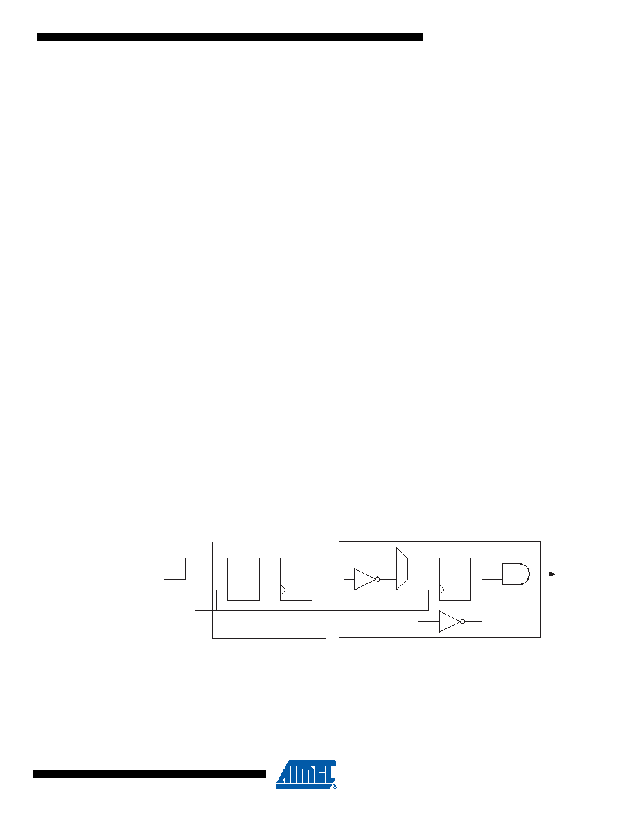
nized (sampled) signal is then passed through the edge detector. Figure 13-1 on page 113
shows a functional equivalent block diagram of the Tn synchronization and edge detector logic.
The registers are clocked at the positive edge of the internal system clock (clk
I/O). The latch is
transparent in the high period of the internal system clock.
The edge detector generates one clk
T0 pulse for each positive (CSn[2:0] = 7) or negative
(CSn[2:0] = 6) edge it detects.
Figure 13-1.
T0 Pin Sampling
The synchronization and edge detector logic introduces a delay of 2.5 to 3.5 system clock cycles
from an edge has been applied to the Tn pin to the counter is updated.
Tn_sync
(To Clock
Select Logic)
Edge Detector
Synchronization
DQ
LE
DQ
Tn
clk
I/O
相關PDF資料 |
PDF描述 |
|---|---|
| MR83C154DXXX-12/883R | 8-BIT, MROM, 12 MHz, MICROCONTROLLER, CQCC44 |
| MQ83C154TXXX-16P883 | 8-BIT, MROM, 16 MHz, MICROCONTROLLER, CQFP44 |
| MR83C154DTXXX-20/883R | 8-BIT, MROM, 20 MHz, MICROCONTROLLER, CQCC44 |
| MC80C52CXXX-30SB | 8-BIT, MROM, 30 MHz, MICROCONTROLLER, CDIP40 |
| MR80C52EXXX-12:D | 8-BIT, MROM, 12 MHz, MICROCONTROLLER, CQCC44 |
相關代理商/技術參數(shù) |
參數(shù)描述 |
|---|---|
| MR80C51BH | 制造商:ROCHESTER 制造商全稱:ROCHESTER 功能描述:CMOS SINGLE - CHIP 8-BIT MICROCOMPUTER 64K program Memory Space |
| MR80C86 | 制造商:INTERSIL 制造商全稱:Intersil Corporation 功能描述:CMOS 16-Bit Microprocessor |
| MR80C86/B | 制造商:Rochester Electronics LLC 功能描述:- Bulk 制造商:Harris Corporation 功能描述:Microprocessor, 16 Bit, 44 Pin, Ceramic, LCC |
| MR80C86-2 | 制造商:INTERSIL 制造商全稱:Intersil Corporation 功能描述:CMOS 16-Bit Microprocessor |
| MR80C86-2/883 | 制造商:Rochester Electronics LLC 功能描述:- Bulk |
發(fā)布緊急采購,3分鐘左右您將得到回復。