- 您現(xiàn)在的位置:買賣IC網(wǎng) > PDF目錄25627 > MR80C32E-16P883 (ATMEL CORP) 8-BIT, 16 MHz, MICROCONTROLLER, CQCC44 PDF資料下載
參數(shù)資料
| 型號: | MR80C32E-16P883 |
| 廠商: | ATMEL CORP |
| 元件分類: | 微控制器/微處理器 |
| 英文描述: | 8-BIT, 16 MHz, MICROCONTROLLER, CQCC44 |
| 封裝: | LCC-44 |
| 文件頁數(shù): | 68/176頁 |
| 文件大小: | 2962K |
| 代理商: | MR80C32E-16P883 |
第1頁第2頁第3頁第4頁第5頁第6頁第7頁第8頁第9頁第10頁第11頁第12頁第13頁第14頁第15頁第16頁第17頁第18頁第19頁第20頁第21頁第22頁第23頁第24頁第25頁第26頁第27頁第28頁第29頁第30頁第31頁第32頁第33頁第34頁第35頁第36頁第37頁第38頁第39頁第40頁第41頁第42頁第43頁第44頁第45頁第46頁第47頁第48頁第49頁第50頁第51頁第52頁第53頁第54頁第55頁第56頁第57頁第58頁第59頁第60頁第61頁第62頁第63頁第64頁第65頁第66頁第67頁當(dāng)前第68頁第69頁第70頁第71頁第72頁第73頁第74頁第75頁第76頁第77頁第78頁第79頁第80頁第81頁第82頁第83頁第84頁第85頁第86頁第87頁第88頁第89頁第90頁第91頁第92頁第93頁第94頁第95頁第96頁第97頁第98頁第99頁第100頁第101頁第102頁第103頁第104頁第105頁第106頁第107頁第108頁第109頁第110頁第111頁第112頁第113頁第114頁第115頁第116頁第117頁第118頁第119頁第120頁第121頁第122頁第123頁第124頁第125頁第126頁第127頁第128頁第129頁第130頁第131頁第132頁第133頁第134頁第135頁第136頁第137頁第138頁第139頁第140頁第141頁第142頁第143頁第144頁第145頁第146頁第147頁第148頁第149頁第150頁第151頁第152頁第153頁第154頁第155頁第156頁第157頁第158頁第159頁第160頁第161頁第162頁第163頁第164頁第165頁第166頁第167頁第168頁第169頁第170頁第171頁第172頁第173頁第174頁第175頁第176頁
16
2535J–AVR–08/10
ATtiny13
The 32 general purpose working registers, 64 I/O Registers, and the 64 bytes of internal data
SRAM in the ATtiny13 are all accessible through all these addressing modes. The Register File
is described in “General Purpose Register File” on page 10.
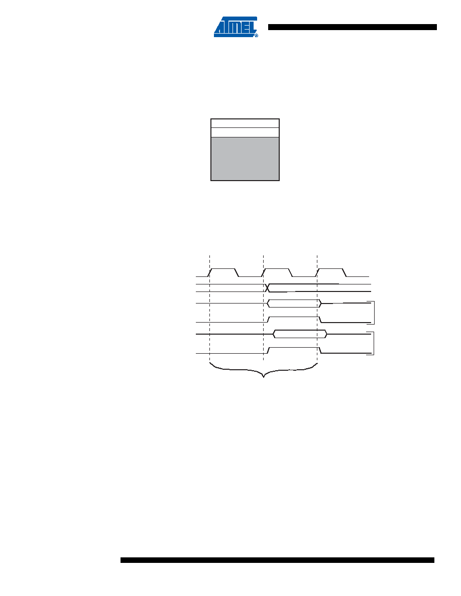
Figure 5-2.
Data Memory Map
5.2.1
Data Memory Access Times
This section describes the general access timing concepts for internal memory access. The
Figure 5-3.
On-chip Data SRAM Access Cycles
5.3
EEPROM Data Memory
The ATtiny13 contains 64 bytes of data EEPROM memory. It is organized as a separate data
space, in which single bytes can be read and written. The EEPROM has an endurance of at
least 100,000 write/erase cycles. The access between the EEPROM and the CPU is described
in the following, specifying the EEPROM Address Registers, the EEPROM Data Register, and
the EEPROM Control Register. For a detailed description of Serial data downloading to the
EEPROM, see page 105.
5.3.1
EEPROM Read/Write Access
The EEPROM Access Registers are accessible in the I/O space.
32 Registers
64 I/O Registers
Internal SRAM
(64 x 8)
0x0000 - 0x001F
0x0020 - 0x005F
0x009F
0x0060
Data Memory
clk
WR
RD
Data
Address
Address valid
T1
T2
T3
Compute Address
Read
Wr
ite
CPU
Memory Access Instruction
Next Instruction
發(fā)布緊急采購,3分鐘左右您將得到回復(fù)。