- 您現(xiàn)在的位置:買賣IC網(wǎng) > PDF目錄384749 > MR16R082CGBN1-CK8 (SAMSUNG SEMICONDUCTOR CO. LTD.) RAMBUS MODULE PDF資料下載
參數(shù)資料
| 型號(hào): | MR16R082CGBN1-CK8 |
| 廠商: | SAMSUNG SEMICONDUCTOR CO. LTD. |
| 英文描述: | RAMBUS MODULE |
| 中文描述: | Rambus的模塊 |
| 文件頁(yè)數(shù): | 4/4頁(yè) |
| 文件大小: | 37K |
| 代理商: | MR16R082CGBN1-CK8 |
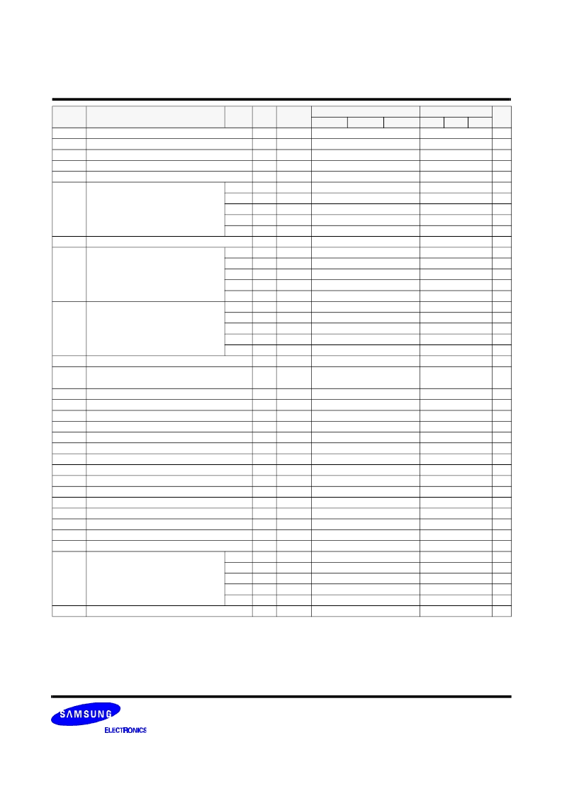
SERIAL PRESENCE DETECT
MR16R0824(6/8/C/G)BN1
RAMBUS MODULE
- 4 -
Version 1.1 Oct. 2000
<Notes>
1. Please refer to Look-Up Table (LUT) in the Direct Rambus
TM
SPD specification 1.0
2. It is reserved to future use (RFU).
3. Unit is not available ( n/a).
4. These bytes are programmed by code of Date Week & Date Year with binary format.
5. These bytes are programmed by Samsung’s own Module Assembly Serial # system. All modules may have unique serial #.
91
92
93
94
Module Manufacturer Revision Code (PCB)
...... Component Manufacturer Revision Code
Module Manufacturing Year
Module Manufacturing Week
Module Serial Number
Number of Devices on Module
8
8
8
8
32
6
6
6
6
6
8
8
8
8
8
8
8
8
8
8
8
16
n/a
n/a
n/a
n/a
n/a
1
31h
42h
-
-
-
04h
06h
08h
0Ch
10h
10h
0Fh
3Fh
FFh
FFh
FFh
00h
00h
00h
0Fh
FFh
00h
3
3
B (B die)
-
-
-
4
6
8
12
16
16bits
3, 4
3, 4
3, 5
95~98
99
4d
6d
8d
12d
16d
devices
devices
devices
devices
devices
bits
bits
bits
bits
bits
bits
bits
bits
bits
bits
bits
bits
100
101
Module Data Width
Devices Enables
4d
6d
8d
12d
16d
4d
6d
8d
12d
16d
All 4 devices are enabled
All 6 devices are enabled
All 8 devices are enabled
All 12 devices are enabled
All 16 devices are enabled
All 4 devices are enabled
All 6 devices are enabled
All 8 devices are enabled
All 12 devices are enabled
All 16 devices are enabled
-
102
...... Devices Enables
103~104 ...... Devices Enables
105
Module Vdd[3:0],
Module Voltage Interface Level[3:0]
4,4
LUT
2.5V, 1.8V Vterm
10h
1
106
Module Vdd Tolerance
107~113 Reserved
114
CDLY0/1 for tCDLY=3
115
CDLY0/1 for tCDLY=4
116
CDLY0/1 for tCDLY=5
117
CDLY0/1 for tCDLY=6
118
CDLY0/1 for tCDLY=7
119
CDLY0/1 for tCDLY=8
120
CDLY0/1 for tCDLY=9
121
CDLY0/1 for tCDLY=10
122
CDLY0/1 for tCDLY=11
123
CDLY0/1 for tCDLY=12
124
CDLY0/1 for tCDLY=13
125
CDLY0/1 for tCDLY=14
126
CDLY0/1 for tCDLY=15
127
Checksum for Bytes 99 ~ 126
8
56
8
8
8
8
8
8
8
8
8
8
8
8
8
8
8
8
8
8
-
LUT
-
t
CYCLE
t
CYCLE
t
CYCLE
t
CYCLE
t
CYCLE
t
CYCLE
t
CYCLE
t
CYCLE
t
CYCLE
t
CYCLE
t
CYCLE
t
CYCLE
t
CYCLE
n/a
n/a
n/a
n/a
n/a
-
5% DC, 2% AC
-
-
-
3 / 0
3 / 1
3 / 2
4 / 2
5 / 2
-
-
-
-
-
-
-
-
-
-
-
-
52h
00h
00h
00h
30h
31h
32h
42h
52h
00h
00h
00h
00h
00h
00h
ACh
DEh
A0h
B3h
A7h
1
4d
6d
8d
12d
16d
3
3
128 +
Open for Customer Use
Undefined
Byte #
(Dec)
Described Function
Option
Field
Width
Units
Supported Function
K8
K7
Hex Value
K7
Note
G6
K8
G6
相關(guān)PDF資料 |
PDF描述 |
|---|---|
| MR16R0824BN1 | RAMBUS MODULE |
| MR16R0824BN1-CG6 | RAMBUS MODULE |
| MR16R0824BN1-CK7 | RAMBUS MODULE |
| MR16R0824BN1-CK8 | RAMBUS MODULE |
| MR16R0826BN1 | RAMBUS MODULE |
相關(guān)代理商/技術(shù)參數(shù) |
參數(shù)描述 |
|---|---|
| MR16R082GAN1-CK800 | 制造商:Samsung SDI 功能描述:INQ# 76-51459 |
| MR16R1622 | 制造商:SAMSUNG 制造商全稱:Samsung semiconductor 功能描述:Key Timing Parameters |
| MR16R16224DF0 | 制造商:SAMSUNG 制造商全稱:Samsung semiconductor 功能描述:Key Timing Parameters |
| MR16R16228DF0 | 制造商:SAMSUNG 制造商全稱:Samsung semiconductor 功能描述:Key Timing Parameters |
| MR16R1622AF0 | 制造商:SAMSUNG 制造商全稱:Samsung semiconductor 功能描述:(16Mx16)x2(4/8/16)pcs RIMM Module based on 256Mb A-die, 32s banks,16K/32ms Ref, 2.5V |
發(fā)布緊急采購(gòu),3分鐘左右您將得到回復(fù)。