- 您現(xiàn)在的位置:買賣IC網(wǎng) > PDF目錄45379 > MQ83C154TXXX-16P883 (ATMEL CORP) 8-BIT, MROM, 16 MHz, MICROCONTROLLER, CQFP44 PDF資料下載
參數(shù)資料
| 型號(hào): | MQ83C154TXXX-16P883 |
| 廠商: | ATMEL CORP |
| 元件分類: | 微控制器/微處理器 |
| 英文描述: | 8-BIT, MROM, 16 MHz, MICROCONTROLLER, CQFP44 |
| 封裝: | CERAMIC, QFP-44 |
| 文件頁數(shù): | 6/286頁 |
| 文件大小: | 9413K |
| 代理商: | MQ83C154TXXX-16P883 |
第1頁第2頁第3頁第4頁第5頁當(dāng)前第6頁第7頁第8頁第9頁第10頁第11頁第12頁第13頁第14頁第15頁第16頁第17頁第18頁第19頁第20頁第21頁第22頁第23頁第24頁第25頁第26頁第27頁第28頁第29頁第30頁第31頁第32頁第33頁第34頁第35頁第36頁第37頁第38頁第39頁第40頁第41頁第42頁第43頁第44頁第45頁第46頁第47頁第48頁第49頁第50頁第51頁第52頁第53頁第54頁第55頁第56頁第57頁第58頁第59頁第60頁第61頁第62頁第63頁第64頁第65頁第66頁第67頁第68頁第69頁第70頁第71頁第72頁第73頁第74頁第75頁第76頁第77頁第78頁第79頁第80頁第81頁第82頁第83頁第84頁第85頁第86頁第87頁第88頁第89頁第90頁第91頁第92頁第93頁第94頁第95頁第96頁第97頁第98頁第99頁第100頁第101頁第102頁第103頁第104頁第105頁第106頁第107頁第108頁第109頁第110頁第111頁第112頁第113頁第114頁第115頁第116頁第117頁第118頁第119頁第120頁第121頁第122頁第123頁第124頁第125頁第126頁第127頁第128頁第129頁第130頁第131頁第132頁第133頁第134頁第135頁第136頁第137頁第138頁第139頁第140頁第141頁第142頁第143頁第144頁第145頁第146頁第147頁第148頁第149頁第150頁第151頁第152頁第153頁第154頁第155頁第156頁第157頁第158頁第159頁第160頁第161頁第162頁第163頁第164頁第165頁第166頁第167頁第168頁第169頁第170頁第171頁第172頁第173頁第174頁第175頁第176頁第177頁第178頁第179頁第180頁第181頁第182頁第183頁第184頁第185頁第186頁第187頁第188頁第189頁第190頁第191頁第192頁第193頁第194頁第195頁第196頁第197頁第198頁第199頁第200頁第201頁第202頁第203頁第204頁第205頁第206頁第207頁第208頁第209頁第210頁第211頁第212頁第213頁第214頁第215頁第216頁第217頁第218頁第219頁第220頁第221頁第222頁第223頁第224頁第225頁第226頁第227頁第228頁第229頁第230頁第231頁第232頁第233頁第234頁第235頁第236頁第237頁第238頁第239頁第240頁第241頁第242頁第243頁第244頁第245頁第246頁第247頁第248頁第249頁第250頁第251頁第252頁第253頁第254頁第255頁第256頁第257頁第258頁第259頁第260頁第261頁第262頁第263頁第264頁第265頁第266頁第267頁第268頁第269頁第270頁第271頁第272頁第273頁第274頁第275頁第276頁第277頁第278頁第279頁第280頁第281頁第282頁第283頁第284頁第285頁第286頁
103
8183F–AVR–06/12
ATtiny24A/44A/84A
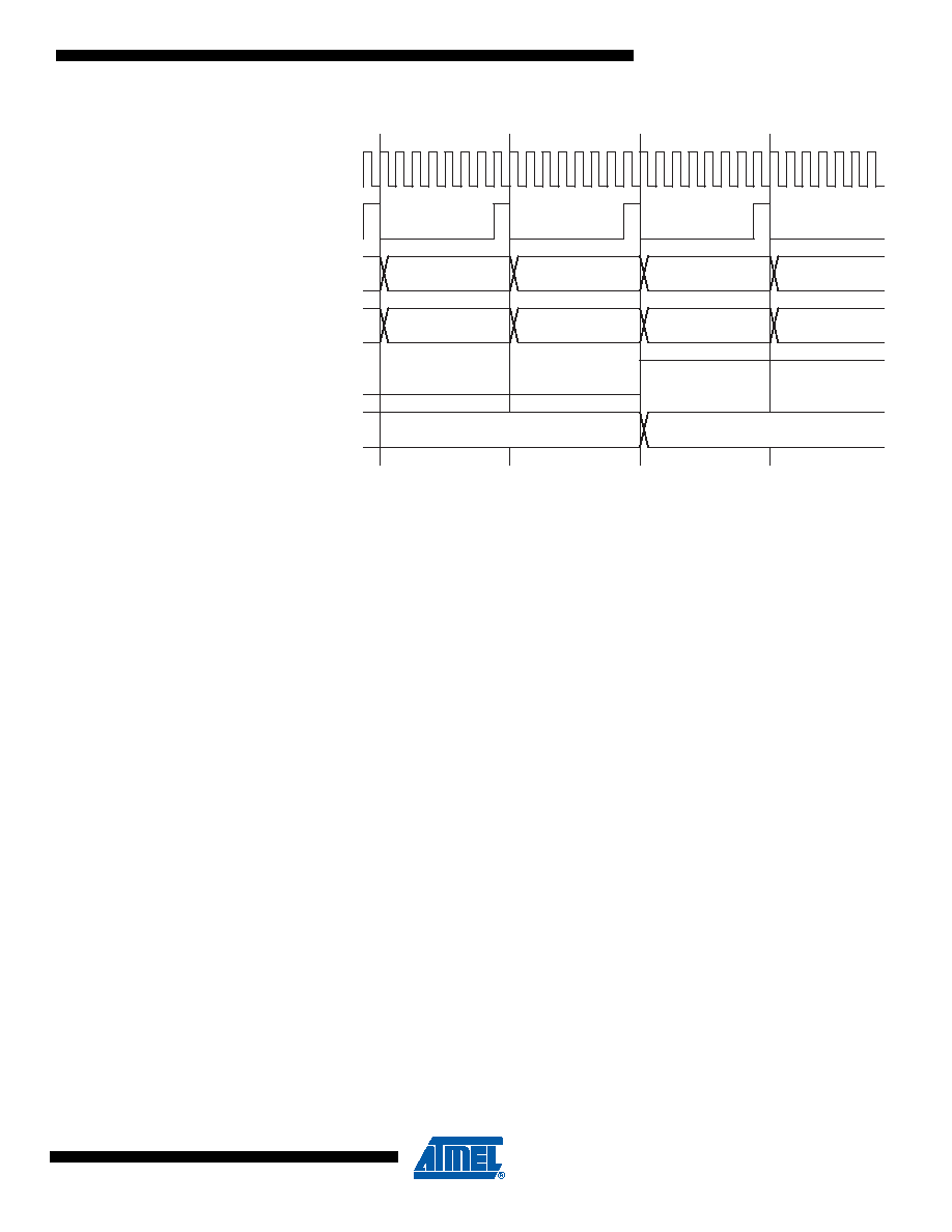
Figure 12-13.
Timer/Counter Timing Diagram, with Prescaler (f
clk_I/O/8)
12.10 Accessing 16-bit Registers
The TCNT1, OCR1A/B, and ICR1 are 16-bit registers that can be accessed by the AVR CPU via
the 8-bit data bus. The 16-bit register must be byte accessed using two read or write operations.
Each 16-bit timer has a single 8-bit register for temporary storing of the high byte of the 16-bit
access. The same temporary register is shared between all 16-bit registers within each 16-bit
timer. Accessing the low byte triggers the 16-bit read or write operation. When the low byte of a
16-bit register is written by the CPU, the high byte stored in the temporary register, and the low
byte written are both copied into the 16-bit register in the same clock cycle. When the low byte of
a 16-bit register is read by the CPU, the high byte of the 16-bit register is copied into the tempo-
rary register in the same clock cycle as the low byte is read.
Not all 16-bit accesses uses the temporary register for the high byte. Reading the OCR1A/B 16-
bit registers does not involve using the temporary register.
To do a 16-bit write, the high byte must be written before the low byte. For a 16-bit read, the low
byte must be read before the high byte.
The following code examples show how to access the 16-bit timer registers assuming that no
interrupts updates the temporary register. The same principle can be used directly for accessing
the OCR1A/B and ICR1 Registers. Note that when using “C”, the compiler handles the 16-bit
access.
TOVn(FPWM)
and ICF n(if used
as TOP)
OCRnx
(Update at TOP)
TCNTn
(CTC and FPWM)
TCNTn
(PC and PFC PWM)
TOP - 1
TOP
TOP - 1
TOP - 2
Old OCRnx Value
New OCRnx Value
TOP - 1
TOP
BOTTOM
BOTTOM + 1
clk
I/O
clk
Tn
(clk
I/O/8)
相關(guān)PDF資料 |
PDF描述 |
|---|---|
| MR83C154DTXXX-20/883R | 8-BIT, MROM, 20 MHz, MICROCONTROLLER, CQCC44 |
| MC80C52CXXX-30SB | 8-BIT, MROM, 30 MHz, MICROCONTROLLER, CDIP40 |
| MR80C52EXXX-12:D | 8-BIT, MROM, 12 MHz, MICROCONTROLLER, CQCC44 |
| MR80C52EXXX-25SHXXX:RD | 8-BIT, MROM, 25 MHz, MICROCONTROLLER, CQCC44 |
| MQ80C52EXXX-12SHXXX:D | 8-BIT, MROM, 12 MHz, MICROCONTROLLER, CQFP44 |
相關(guān)代理商/技術(shù)參數(shù) |
參數(shù)描述 |
|---|---|
| MQ86 | 制造商:TE Connectivity 功能描述: |
| MQ8797BH | 制造商:Rochester Electronics LLC 功能描述:- Bulk 制造商:Intel 功能描述: |
| MQ87C196KC/R | 制造商:Rochester Electronics LLC 功能描述: |
| MQ87C196KD-16/B | 制造商:Rochester Electronics LLC 功能描述: |
| MQ87C196KD-20/R | 制造商:Rochester Electronics LLC 功能描述: |
發(fā)布緊急采購,3分鐘左右您將得到回復(fù)。