- 您現(xiàn)在的位置:買賣IC網(wǎng) > PDF目錄98028 > MPM22CUC450B (INTEL CORP) 32-BIT, 450 MHz, MICROPROCESSOR, XMA PDF資料下載
參數(shù)資料
| 型號(hào): | MPM22CUC450B |
| 廠商: | INTEL CORP |
| 元件分類: | 微控制器/微處理器 |
| 英文描述: | 32-BIT, 450 MHz, MICROPROCESSOR, XMA |
| 封裝: | MMC-2 |
| 文件頁(yè)數(shù): | 32/64頁(yè) |
| 文件大小: | 778K |
| 代理商: | MPM22CUC450B |
第1頁(yè)第2頁(yè)第3頁(yè)第4頁(yè)第5頁(yè)第6頁(yè)第7頁(yè)第8頁(yè)第9頁(yè)第10頁(yè)第11頁(yè)第12頁(yè)第13頁(yè)第14頁(yè)第15頁(yè)第16頁(yè)第17頁(yè)第18頁(yè)第19頁(yè)第20頁(yè)第21頁(yè)第22頁(yè)第23頁(yè)第24頁(yè)第25頁(yè)第26頁(yè)第27頁(yè)第28頁(yè)第29頁(yè)第30頁(yè)第31頁(yè)當(dāng)前第32頁(yè)第33頁(yè)第34頁(yè)第35頁(yè)第36頁(yè)第37頁(yè)第38頁(yè)第39頁(yè)第40頁(yè)第41頁(yè)第42頁(yè)第43頁(yè)第44頁(yè)第45頁(yè)第46頁(yè)第47頁(yè)第48頁(yè)第49頁(yè)第50頁(yè)第51頁(yè)第52頁(yè)第53頁(yè)第54頁(yè)第55頁(yè)第56頁(yè)第57頁(yè)第58頁(yè)第59頁(yè)第60頁(yè)第61頁(yè)第62頁(yè)第63頁(yè)第64頁(yè)
Pentium
III Processor Mobile Module MMC-2
32
Datasheet
245304-004
5.3.2
Voltage Regulator Control
The VR_ON pin on the connector allows a 3.3-V signal to control the voltage regulator. The
system manufacturer can use this signal to turn the voltage regulator on or off. VR_ON should be
controlled as a function of the same signal (SUSB#) used to control the system’s switched 5.0-V
and 3.3-V power planes. The PIIX4E/M defines Suspend B as the Power Management state in
which power is physically removed from the processor and the voltage regulator. In this state, the
SUSB# pin on the PIIX4E/M controls these power planes. The mobile module provides the
VR_PWRGD signal, which indicates that the voltage regulator power is operating at a stable
voltage level. The system manufacturer should use this signal on the system electronics to control
power inputs and to gate PWROK to the PIIX4E/M South Bridge. Table 22 provides the detailed
definitions and sequences of the voltage signals.
The following list includes additional specifications and clarifications of the power sequence
timing and Figure 6 provides an illustration.
1. The VR_ON signal may only be asserted to a logical high by a digital signal after V_DC
≥
7.5V, V_5
≥ 4.5V, and V_3 ≥ 3.0V.
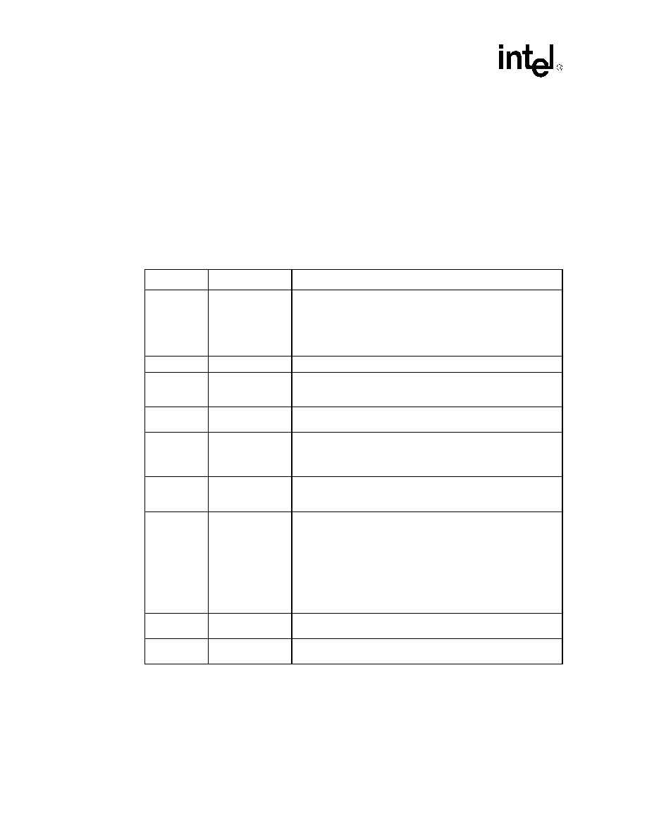
Table 22. Voltage Signal Definitions and Sequences
Signal
Source
Definitions and Sequences
V_DC
System Electronics
V_DC is required to be between 7.5V and 21.0V DC and is driven by
the system electronics’ power supply. V_DC powers the Pentium III
processor mobile module DC-to-DC converter for the processor core
and I/O voltages.
The mobile module cannot be hot inserted or removed while
V_DC is powered on.
V_5
System Electronics
V_5 is supplied by the system electronics for the voltage regulator.
V_3
System Electronics
V_3 is supplied by the system electronics for the 82443BX and powers
the mobile module’s linear regulators for generating the V_CLK and
V_CPUPU voltage rails. It stays on during suspend.
V_3S
System Electronics
V_3S is supplied by the system electronics, and V_3S is shut off
during suspend.
VR_ON
System Electronics
VR_ON is a 3.3-V signal that enables the voltage regulator circuit.
When driven active high, the voltage regulator circuit is activated. The
signal driving VR_ON should be a digital signal with a rise and fall time
of less than or equal to 1
S. (V
IL (max)= 0.4V, VIH (min)= 3.0V.)
V_CORE
Module
A result of VR_ON being asserted, V_CORE is an output of the DC-
DC regulator on the mobile module and is driven to the core voltage of
the processor.
VR_PWRGD
Module
Upon sampling the voltage level of V_CORE (minus tolerances for
ripple), VR_PWRGD is driven active high. If VR_PWRGD is not
sampled active within 1 second of the assertion of VR_ON, then the
system electronics should deassert VR_ON. After V_CORE is
stabilized, VR_PWRGD will assert to logic high (3.3V). This signal
must not be pulled up by the system electronics. VR_PWRGD should
be "logically ANDed" with V_3S to generate the PIIX4E/M input signal,
PWROK. The system electronics should monitor VR_PWRGD to verify
that it is asserted high prior to the active high assertion of PIIX4E/M
PWROK.
V_CPUPU
Module
V_CPUPU is 1.5V. The system electronics uses this voltage to power
the PIIX4E/M-to-processor interface circuitry.
V_CLK
Module
V_CLK is 2.5V. The system electronics uses this voltage to power the
HCLK[0:1] drivers for the processor clock.
相關(guān)PDF資料 |
PDF描述 |
|---|---|
| MPQ2222 | 0.5 A, 30 V, 4 CHANNEL, NPN, Si, POWER TRANSISTOR, TO-116 |
| MPQ2222A | 0.5 A, 40 V, 4 CHANNEL, NPN, Si, POWER TRANSISTOR, TO-116 |
| MPQ2484 | 50 mA, 40 V, 4 CHANNEL, NPN, Si, SMALL SIGNAL TRANSISTOR, TO-116 |
| MPQ2483 | 50 mA, 40 V, 4 CHANNEL, NPN, Si, SMALL SIGNAL TRANSISTOR, TO-116 |
| MPQ2907A | 0.6 A, 60 V, 4 CHANNEL, PNP, Si, POWER TRANSISTOR, TO-116 |
相關(guān)代理商/技術(shù)參數(shù) |
參數(shù)描述 |
|---|---|
| MPM-25S | 制造商:MPD 制造商全稱:MicroPower Direct, LLC 功能描述:Universal Input, 25W Miniature, PC Mount AC/DC Power Supplies |
| MPM-25S-05 | 制造商:MPD 制造商全稱:MicroPower Direct, LLC 功能描述:Universal Input, 25W Miniature, PC Mount AC/DC Power Supplies |
| MPM-25S-12 | 制造商:MPD 制造商全稱:MicroPower Direct, LLC 功能描述:Universal Input, 25W Miniature, PC Mount AC/DC Power Supplies |
| MPM-25S-15 | 制造商:MPD 制造商全稱:MicroPower Direct, LLC 功能描述:Universal Input, 25W Miniature, PC Mount AC/DC Power Supplies |
| MPM-25S-24 | 制造商:MPD 制造商全稱:MicroPower Direct, LLC 功能描述:Universal Input, 25W Miniature, PC Mount AC/DC Power Supplies |
發(fā)布緊急采購(gòu),3分鐘左右您將得到回復(fù)。