- 您現(xiàn)在的位置:買(mǎi)賣(mài)IC網(wǎng) > PDF目錄45374 > MPC92432AER2 (INTEGRATED DEVICE TECHNOLOGY INC) 1360 MHz, OTHER CLOCK GENERATOR, PQFP48 PDF資料下載
參數(shù)資料
| 型號(hào): | MPC92432AER2 |
| 廠商: | INTEGRATED DEVICE TECHNOLOGY INC |
| 元件分類(lèi): | 時(shí)鐘產(chǎn)生/分配 |
| 英文描述: | 1360 MHz, OTHER CLOCK GENERATOR, PQFP48 |
| 封裝: | LEAD FREE, LQFP-48 |
| 文件頁(yè)數(shù): | 7/20頁(yè) |
| 文件大小: | 412K |
| 代理商: | MPC92432AER2 |
第1頁(yè)第2頁(yè)第3頁(yè)第4頁(yè)第5頁(yè)第6頁(yè)當(dāng)前第7頁(yè)第8頁(yè)第9頁(yè)第10頁(yè)第11頁(yè)第12頁(yè)第13頁(yè)第14頁(yè)第15頁(yè)第16頁(yè)第17頁(yè)第18頁(yè)第19頁(yè)第20頁(yè)
Advanced Clock Drivers Devices
Freescale Semiconductor
15
MPC92432
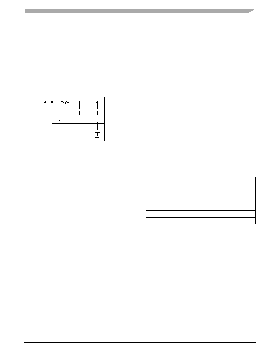
VCC_PLL Filter
The MPC92432 is a mixed analog/digital product. Its
analog circuitry is naturally susceptible to random noise,
especially if this noise is seen on the power supply pins.
Random noise on the VCC_PLL pin impacts the device AC
characteristics. The MPC92432 provides separate power
supplies for the digital circuitry (VCC) and the internal PLL
(VCC_PLL) of the device. The purpose of this design
technique is to isolate the high switching noise digital outputs
from the relatively sensitive internal analog phase-locked
loop. In digital system environments where it is more difficult
to minimize noise on the power supplies a second level of
isolation is recommended: a power supply filter on the
VCC_PLL pin for the MPC92432.
Figure 7. VCC_PLL Power Supply Filter
Figure 7 illustrates a recommended power supply filter
scheme.
The MPC92432 is most susceptible to noise with spectral
content in the 100 kHz to 1 MHz range. Therefore, the filter
should be designed to target this range. The key parameter
that needs to be met in the final filter design is the DC voltage
drop that will be seen between the VCC supply and the
VCC_PLL pin of the MPC92432. From the data sheet, the
VCC_PLL current (the current sourced through the VCC_PLL
pin) is maximum 10 mA, assuming that a minimum of 2.985 V
must be maintained on the VCC_PLL pin. The resistor shown
to meet the
voltage drop criteria. The minimum values for RF and the filter
capacitor CF are defined by the filter characteristics: the RC
filter should provide an attenuation greater than 40 dB for
noise whose spectral content is above 100 kHz. In the
recommended filter shown in Figure 7 the filter cut-off
frequency is around 3.0–4.5 kHz and the noise attenuation at
100 kHz is better than 42 dB.
As the noise frequency crosses the series resonant point
of an individual capacitor its overall impedance begins to look
inductive and thus increases with increasing frequency. The
parallel capacitor combination shown ensures that a low
impedance path to ground exists for frequencies well above
the bandwidth of the PLL.
The On-Chip Crystal Oscillator
The MPC92432 features an integrated on-chip crystal
oscillator to minimize system implementation cost. The
integrated oscillator is a Pierce-type that uses the crystal in
its parallel resonance mode. It is recommended to use a 15
to 20 MHz crystal with a load specification of CL =10pF.
Crystals with a load specification of CL = 20 pF may be used
at the expense of an resulting slightly higher frequency than
specified for the crystal. Externally connected capacitors on
both the XTAL_IN and XTAL_OUT pins are not required but
can be used to fine-tune the crystal frequency as desired.
The crystal, the trace and optional capacitors should be
placed on the board as close as possible to the MPC92432
XTAL_IN and XTAL_OUT pins to reduce crosstalk of active
signals into the oscillator. Short and wide traces further
reduce parasitic inductance and resistance. It is further
recommended to guard the crystal circuit by placing a ground
ring around the traces and oscillator components.
RF = 10–15
VCC
CF = 22 F
10 nF
33...100 nF
VCC_PLL
VCC
MPC92432
7
Table 23. Recommended Crystal Specifications
Parameter
Value
Crystal Cut
Fundamental AT Cut
Resonance Mode
Parallel
Crystal Frequency
16–20 MHz
Shunt Capacitance C0
5–7 pF
Load Capacitance CL
10 pF
Equivalent Series Resistance ESR
20–60
相關(guān)PDF資料 |
PDF描述 |
|---|---|
| MPC92432FAR2 | 1360 MHz, OTHER CLOCK GENERATOR, PQFP48 |
| MPC92439EI | 900 MHz, OTHER CLOCK GENERATOR, PQCC28 |
| MPC92439EI | 900 MHz, OTHER CLOCK GENERATOR, PQCC28 |
| MPC92439EIR2 | 900 MHz, OTHER CLOCK GENERATOR, PQCC28 |
| MPC92439FNR2 | 900 MHz, OTHER CLOCK GENERATOR, PQCC28 |
相關(guān)代理商/技術(shù)參數(shù) |
參數(shù)描述 |
|---|---|
| MPC92432FA | 制造商:MOTOROLA 制造商全稱(chēng):Motorola, Inc 功能描述:1360 MHz Dual Output LVPECL Clock Synthesizer |
| MPC92433 | 制造商:FREESCALE 制造商全稱(chēng):Freescale Semiconductor, Inc 功能描述:1428 MHz Dual Output LVPECL Clock Synthesizer |
| MPC92433AE | 功能描述:時(shí)鐘合成器/抖動(dòng)清除器 FSL 1428MHz Dual Out put LVPECL Clock Syn RoHS:否 制造商:Skyworks Solutions, Inc. 輸出端數(shù)量: 輸出電平: 最大輸出頻率: 輸入電平: 最大輸入頻率:6.1 GHz 電源電壓-最大:3.3 V 電源電壓-最小:2.7 V 封裝 / 箱體:TSSOP-28 封裝:Reel |
| MPC92433AER2 | 功能描述:時(shí)鐘合成器/抖動(dòng)清除器 FSL 1428MHz Dual Out put LVPECL Clock Syn RoHS:否 制造商:Skyworks Solutions, Inc. 輸出端數(shù)量: 輸出電平: 最大輸出頻率: 輸入電平: 最大輸入頻率:6.1 GHz 電源電壓-最大:3.3 V 電源電壓-最小:2.7 V 封裝 / 箱體:TSSOP-28 封裝:Reel |
| MPC92439 | 制造商:IDT 制造商全稱(chēng):Integrated Device Technology 功能描述:900MHz, Low Voltage, LVPECL Clock Syntheesizer |
發(fā)布緊急采購(gòu),3分鐘左右您將得到回復(fù)。