- 您現(xiàn)在的位置:買賣IC網(wǎng) > PDF目錄65817 > MPC9239FNR2 (MOTOROLA INC) 900 MHz, OTHER CLOCK GENERATOR, PQCC28 PDF資料下載
參數(shù)資料
| 型號(hào): | MPC9239FNR2 |
| 廠商: | MOTOROLA INC |
| 元件分類: | 時(shí)鐘產(chǎn)生/分配 |
| 英文描述: | 900 MHz, OTHER CLOCK GENERATOR, PQCC28 |
| 封裝: | PLASTIC, LCC-28 |
| 文件頁數(shù): | 7/9頁 |
| 文件大小: | 136K |
| 代理商: | MPC9239FNR2 |
4
MPC9239
MOTOROLA ADVANCED CLOCK DRIVERS DEVICE DATA
423
Programming the MPC9239
Programming the MPC9239 amounts to properly configuring
the internal PLL dividers to produce the desired synthesized
frequency at the output. The output frequency can be repre-
sented by this formula:
fOUT = (fXTAL ÷ 2) (M 4) ÷ (N 2) or
(1)
fOUT = fXTAL M ÷ N
(2)
where fXTAL is the crystal frequency, M is the PLL feedback-di-
vider and N is the PLL post-divider. The input frequency and the
selection of the feedback divider M is limited by the VCO-fre-
quency range. fXTAL and M must be configured to match the
VCO frequency range of 800 to 1800 MHz in order to achieve
stable PLL operation:
MMIN = fVCO,MIN ÷ (2fXTAL) and
(3)
MMAX = fVCO,MAX ÷ (2fXTAL)
(4)
For instance, the use of a 16 MHz input frequency requires
the configuration of the PLL feedback divider between M = 25
and M = 56. Table 8 shows the usable VCO frequency and M
divider range for other example input frequencies.
Assuming that a 16 MHz input frequency is used, equation (2)
reduces to:
fOUT = 16 M ÷ N
(5)
Substituting N for the four available values for N (1, 2, 4, 8)
yields:
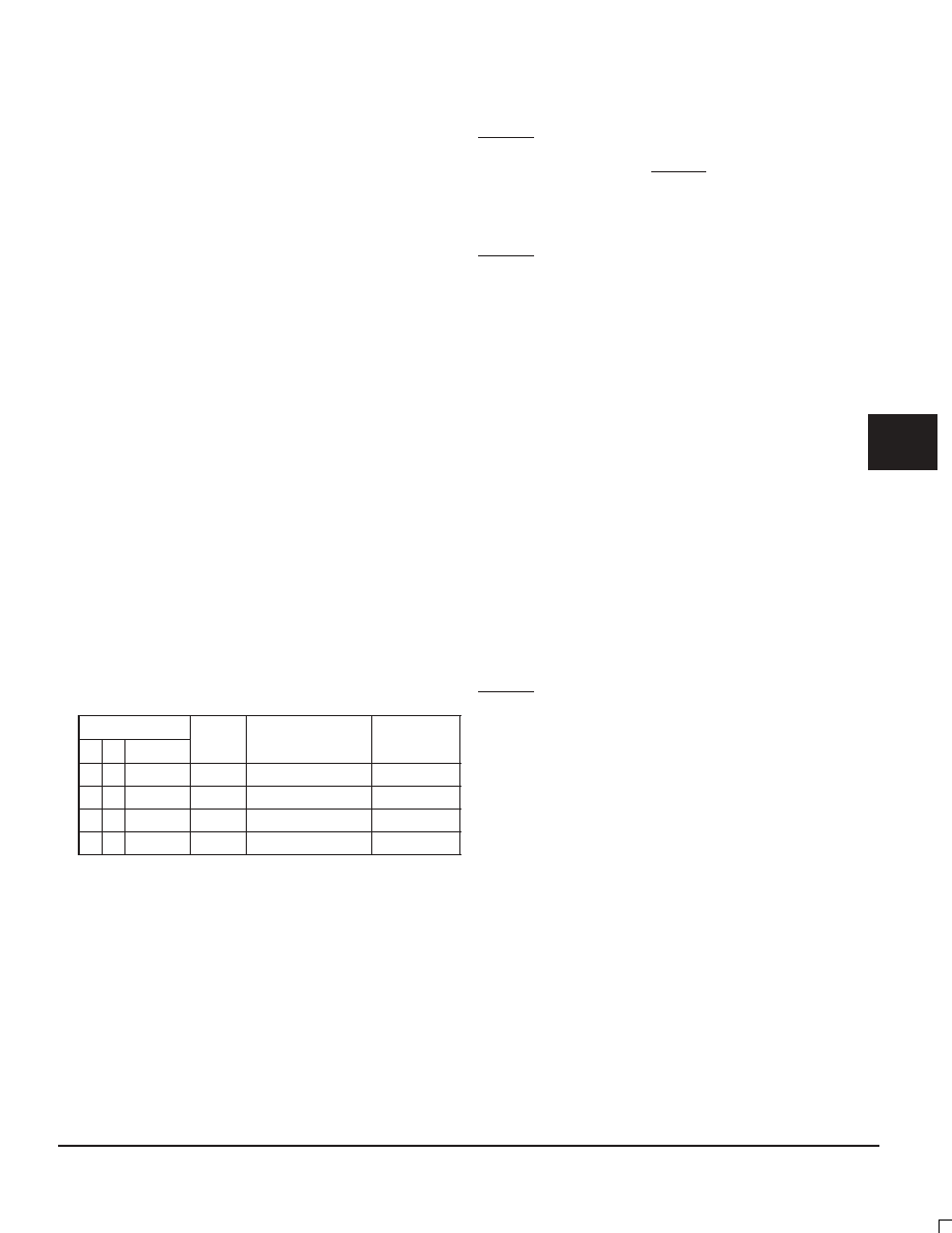
Table 9. Output Frequency Range for fXTAL = 16 MHz
N
FOUT
FOUT range
FOUT step
1
0
Value
OUT
g
OUT
p
0
2
8
M
200-450 MHz
8 MHz
0
1
4
M
100-225 MHz
4 MHz
1
0
8
2
M
50-112.5 MHz
2 MHz
1
16
M
400-900 MHz
16 MHz
Example calculation for an 16 MHz input frequency
For example, if an output frequency of 384 MHz was desired,
the following steps would be taken to identify the appropriate M
and N values. 384 MHz falls within the frequency range set by
an N value of 2, so N[1:0]=00. For N = 2, FOUT = 8
M and M =
FOUT
÷8. Therefore, M = 384 ÷ 8 = 48, so M[6:0] = 0110000.
Following this procedure a user can generate any whole
frequency between 50 MHz and 900 MHz. The size of the
programmable frequency steps will be equal to:
fSTEP = fXTAL ÷ N
(6)
Using the parallel and serial interface
The M and N counters can be loaded either through a parallel
or serial interface. The parallel interface is controlled via the
P_LOAD signal such that a LOW to HIGH transition will latch the
information present on the M[6:0] and N[1:0] inputs into the M
and N counters. When the P_LOAD signal is LOW the input
latches will be transparent and any changes on the M[6:0] and
N[1:0] inputs will affect the FOUT output pair. To use the serial
port the S_CLOCK signal samples the information on the
S_DATA line and loads it into a 12 bit shift register. Note that the
P_LOAD signal must be HIGH for the serial load operation to
function. The Test register is loaded with the first three bits, the
N register with the next two, and the M register with the final
eight bits of the data stream on the S_DATA input. For each
register the most significant bit is loaded first (T2, N1 and M6).
A pulse on the S_LOAD pin after the shift register is fully loaded
will transfer the divide values into the counters. The HIGH to
LOW transition on the S_LOAD input will latch the new divide
values into the counters. Figure 4 illustrates the timing diagram
for both a parallel and a serial load of the MPC9239 synthesizer.
M[6:0] and N[1:0] are normally specified once at power–up
through the parallel interface, and then possibly again through
the serial interface. This approach allows the application to
come up at one frequency and then change or fine–tune the
clock as the ability to control the serial interface becomes
available.
Using the test and diagnosis output TEST
The TEST output provides visibility for one of the several
internal nodes as determined by the T[2:0] bits in the serial
configuration stream. It is not configurable through the parallel
interface. Although it is possible to select the node that
represents FOUT, the LVCMOS output is not able to toggle fast
enough for higher output frequencies and should only be used
for test and dignosis.
The T2, T1 and T0 control bits are preset to ‘000’ when
P_LOAD is LOW so that the PECL FOUT outputs are as
jitter–free as possible. Any active signal on the TEST output pin
will have detrimental affects on the jitter of the PECL output pair.
In normal operations, jitter specifications are only guaranteed
if the TEST output is static. The serial configuration port can be
used to select one of the alternate functions for this pin.
Most of the signals available on the TEST output pin are
useful only for performance verification of the MPC9239 itself.
However, the PLL bypass mode may be of interest at the board
level for functional debug. When T[2:0] is set to 110 the
MPC9239 is placed in PLL bypass mode. In this mode the
S_CLOCK input is fed directly into the M and N dividers. The N
divider drives the FOUT differential pair and the M counter
drives the TEST output pin. In this mode the S_CLOCK input
could be used for low speed board level functional test or debug.
Bypassing the PLL and driving FOUT directly gives the user
more control on the test clocks sent through the clocktree
shows the functional setup of the PLL bypass mode. Because
the S_CLOCK is a CMOS level the input frequency is limited to
200 MHz. This means the fastest the FOUT pin can be toggled
via the S_CLOCK is 100 MHz as the divide ratio of the Post-PLL
divider is 2 (if N = 1). Note that the M counter output on the TEST
output will not be a 50% duty cycle.
相關(guān)PDF資料 |
PDF描述 |
|---|---|
| MPC9239FN | 900 MHz, OTHER CLOCK GENERATOR, PQCC28 |
| MPC9259FA | 900 MHz, OTHER CLOCK GENERATOR, PQFP32 |
| MPC926508SDR2 | 133.33 MHz, OTHER CLOCK GENERATOR, PDSO20 |
| MPC926508SDR2 | 133.33 MHz, OTHER CLOCK GENERATOR, PDSO20 |
| MPC950FAR2 | 180 MHz, PROC SPECIFIC CLOCK GENERATOR, PQFP32 |
相關(guān)代理商/技術(shù)參數(shù) |
參數(shù)描述 |
|---|---|
| MPC92429 | 制造商:MOTOROLA 制造商全稱:Motorola, Inc 功能描述:400 MHz Low Voltage PECL Clock Synthesizer |
| MPC92429AC | 功能描述:時(shí)鐘合成器/抖動(dòng)清除器 RoHS:否 制造商:Skyworks Solutions, Inc. 輸出端數(shù)量: 輸出電平: 最大輸出頻率: 輸入電平: 最大輸入頻率:6.1 GHz 電源電壓-最大:3.3 V 電源電壓-最小:2.7 V 封裝 / 箱體:TSSOP-28 封裝:Reel |
| MPC92429ACR2 | 功能描述:時(shí)鐘合成器/抖動(dòng)清除器 RoHS:否 制造商:Skyworks Solutions, Inc. 輸出端數(shù)量: 輸出電平: 最大輸出頻率: 輸入電平: 最大輸入頻率:6.1 GHz 電源電壓-最大:3.3 V 電源電壓-最小:2.7 V 封裝 / 箱體:TSSOP-28 封裝:Reel |
| MPC92429EI | 功能描述:時(shí)鐘合成器/抖動(dòng)清除器 RoHS:否 制造商:Skyworks Solutions, Inc. 輸出端數(shù)量: 輸出電平: 最大輸出頻率: 輸入電平: 最大輸入頻率:6.1 GHz 電源電壓-最大:3.3 V 電源電壓-最小:2.7 V 封裝 / 箱體:TSSOP-28 封裝:Reel |
| MPC92429EIR2 | 功能描述:時(shí)鐘合成器/抖動(dòng)清除器 RoHS:否 制造商:Skyworks Solutions, Inc. 輸出端數(shù)量: 輸出電平: 最大輸出頻率: 輸入電平: 最大輸入頻率:6.1 GHz 電源電壓-最大:3.3 V 電源電壓-最小:2.7 V 封裝 / 箱體:TSSOP-28 封裝:Reel |
發(fā)布緊急采購,3分鐘左右您將得到回復(fù)。