- 您現(xiàn)在的位置:買(mǎi)賣(mài)IC網(wǎng) > PDF目錄25630 > MPC8548CVTATJB (FREESCALE SEMICONDUCTOR INC) 32-BIT, 1200 MHz, MICROPROCESSOR, PBGA783 PDF資料下載
參數(shù)資料
| 型號(hào): | MPC8548CVTATJB |
| 廠商: | FREESCALE SEMICONDUCTOR INC |
| 元件分類(lèi): | 微控制器/微處理器 |
| 英文描述: | 32-BIT, 1200 MHz, MICROPROCESSOR, PBGA783 |
| 封裝: | 29 X 29 MM, 1 MM PITCH, FLIP CHIP, LEAD FREE, PLASTIC, BGA-783 |
| 文件頁(yè)數(shù): | 85/142頁(yè) |
| 文件大小: | 1504K |
| 代理商: | MPC8548CVTATJB |
第1頁(yè)第2頁(yè)第3頁(yè)第4頁(yè)第5頁(yè)第6頁(yè)第7頁(yè)第8頁(yè)第9頁(yè)第10頁(yè)第11頁(yè)第12頁(yè)第13頁(yè)第14頁(yè)第15頁(yè)第16頁(yè)第17頁(yè)第18頁(yè)第19頁(yè)第20頁(yè)第21頁(yè)第22頁(yè)第23頁(yè)第24頁(yè)第25頁(yè)第26頁(yè)第27頁(yè)第28頁(yè)第29頁(yè)第30頁(yè)第31頁(yè)第32頁(yè)第33頁(yè)第34頁(yè)第35頁(yè)第36頁(yè)第37頁(yè)第38頁(yè)第39頁(yè)第40頁(yè)第41頁(yè)第42頁(yè)第43頁(yè)第44頁(yè)第45頁(yè)第46頁(yè)第47頁(yè)第48頁(yè)第49頁(yè)第50頁(yè)第51頁(yè)第52頁(yè)第53頁(yè)第54頁(yè)第55頁(yè)第56頁(yè)第57頁(yè)第58頁(yè)第59頁(yè)第60頁(yè)第61頁(yè)第62頁(yè)第63頁(yè)第64頁(yè)第65頁(yè)第66頁(yè)第67頁(yè)第68頁(yè)第69頁(yè)第70頁(yè)第71頁(yè)第72頁(yè)第73頁(yè)第74頁(yè)第75頁(yè)第76頁(yè)第77頁(yè)第78頁(yè)第79頁(yè)第80頁(yè)第81頁(yè)第82頁(yè)第83頁(yè)第84頁(yè)當(dāng)前第85頁(yè)第86頁(yè)第87頁(yè)第88頁(yè)第89頁(yè)第90頁(yè)第91頁(yè)第92頁(yè)第93頁(yè)第94頁(yè)第95頁(yè)第96頁(yè)第97頁(yè)第98頁(yè)第99頁(yè)第100頁(yè)第101頁(yè)第102頁(yè)第103頁(yè)第104頁(yè)第105頁(yè)第106頁(yè)第107頁(yè)第108頁(yè)第109頁(yè)第110頁(yè)第111頁(yè)第112頁(yè)第113頁(yè)第114頁(yè)第115頁(yè)第116頁(yè)第117頁(yè)第118頁(yè)第119頁(yè)第120頁(yè)第121頁(yè)第122頁(yè)第123頁(yè)第124頁(yè)第125頁(yè)第126頁(yè)第127頁(yè)第128頁(yè)第129頁(yè)第130頁(yè)第131頁(yè)第132頁(yè)第133頁(yè)第134頁(yè)第135頁(yè)第136頁(yè)第137頁(yè)第138頁(yè)第139頁(yè)第140頁(yè)第141頁(yè)第142頁(yè)
MPC8548E PowerQUICC III Integrated Processor Hardware Specifications, Rev. 5
Freescale Semiconductor
47
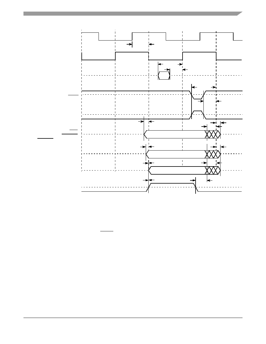
Local Bus
Figure 24. Local Bus Signals (PLL Bypass Mode)
NOTE
In PLL bypass mode, LCLK[n] is the inverted version of the internal clock
with the delay of tLBKHKT. In this mode, signals are launched at the rising edge
of the internal clock and are captured at falling edge of the internal clock
with the exception of LGTA/LUPWAIT (which is captured on the rising
edge of the internal clock).
Output Signals:
LA[27:31]/LBCTL/LBCKE/LOE/
LSDA10/LSDWE/LSDRAS/
LSDCAS/LSDDQM[0:3]
tLBKLOV2
LCLK[
n]
Input Signals:
LAD[0:31]/LDP[0:3]
Output (Data) Signals:
LAD[0:31]/LDP[0:3]
LALE
tLBIXKH1
Input Signal:
LGTA
Output (Address) Signal:
LAD[0:31]
tLBIVKH1
tLBIXKL2
tLBIVKL2
tLBKLOX1
tLBKLOZ2
tLBOTOT
Internal Launch/Capture Clock
tLBKLOX2
tLBKLOV1
tLBKLOV3
tLBKLOZ1
tLBKHKT
tLBKLOV4
LUPWAIT
發(fā)布緊急采購(gòu),3分鐘左右您將得到回復(fù)。