- 您現(xiàn)在的位置:買賣IC網(wǎng) > PDF目錄17039 > MPC8536E-ANDROID (Freescale Semiconductor)HARDWARE/SOFTWARE ANDROID OS PDF資料下載
參數(shù)資料
| 型號: | MPC8536E-ANDROID |
| 廠商: | Freescale Semiconductor |
| 文件頁數(shù): | 124/126頁 |
| 文件大小: | 0K |
| 描述: | HARDWARE/SOFTWARE ANDROID OS |
| 標(biāo)準(zhǔn)包裝: | 1 |
| 系列: | PowerQUICC ™ |
| 類型: | MPU |
| 適用于相關(guān)產(chǎn)品: | MPC8536 |
| 所含物品: | 板 |
第1頁第2頁第3頁第4頁第5頁第6頁第7頁第8頁第9頁第10頁第11頁第12頁第13頁第14頁第15頁第16頁第17頁第18頁第19頁第20頁第21頁第22頁第23頁第24頁第25頁第26頁第27頁第28頁第29頁第30頁第31頁第32頁第33頁第34頁第35頁第36頁第37頁第38頁第39頁第40頁第41頁第42頁第43頁第44頁第45頁第46頁第47頁第48頁第49頁第50頁第51頁第52頁第53頁第54頁第55頁第56頁第57頁第58頁第59頁第60頁第61頁第62頁第63頁第64頁第65頁第66頁第67頁第68頁第69頁第70頁第71頁第72頁第73頁第74頁第75頁第76頁第77頁第78頁第79頁第80頁第81頁第82頁第83頁第84頁第85頁第86頁第87頁第88頁第89頁第90頁第91頁第92頁第93頁第94頁第95頁第96頁第97頁第98頁第99頁第100頁第101頁第102頁第103頁第104頁第105頁第106頁第107頁第108頁第109頁第110頁第111頁第112頁第113頁第114頁第115頁第116頁第117頁第118頁第119頁第120頁第121頁第122頁第123頁當(dāng)前第124頁第125頁第126頁
Electrical Characteristics
MPC8536E PowerQUICC III Integrated Processor Hardware Specifications, Rev. 5
Freescale Semiconductor
97
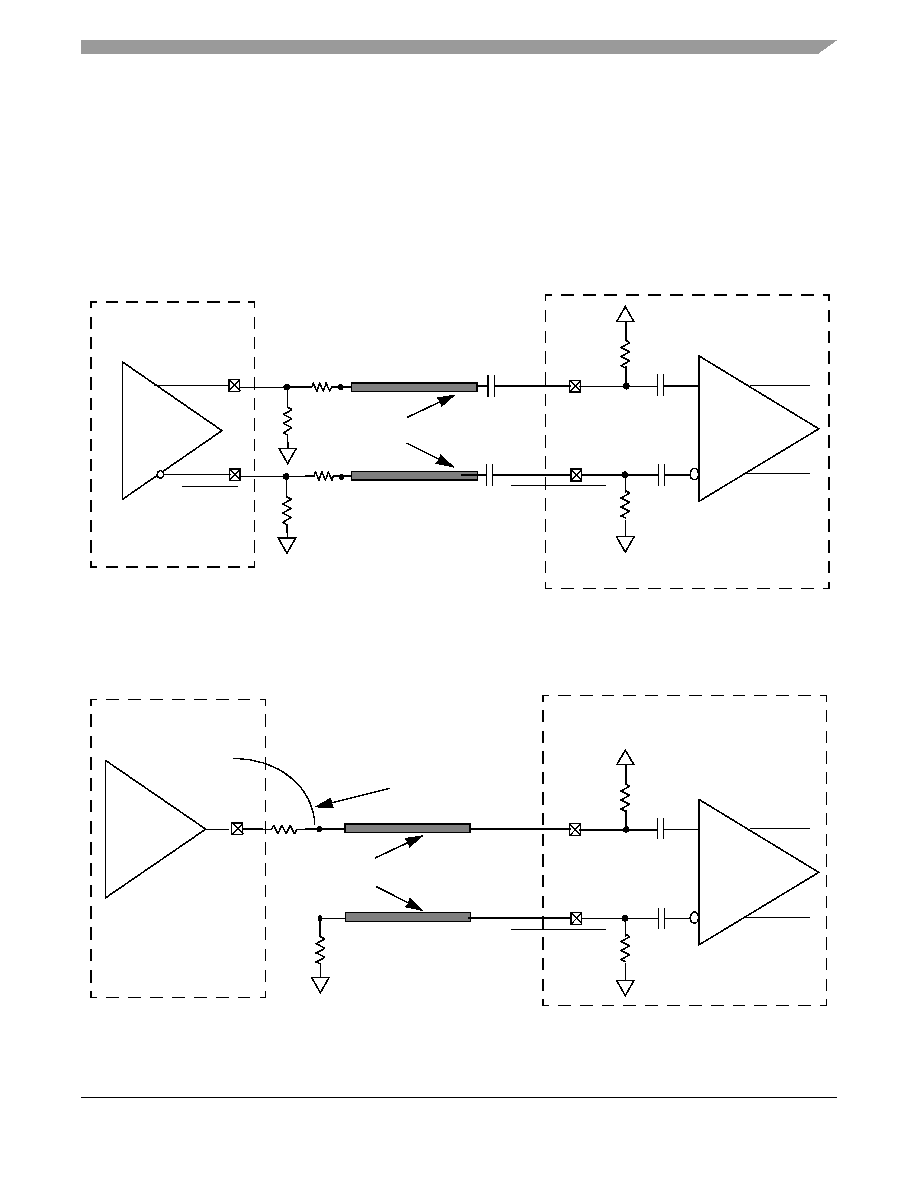
This figure shows the SerDes reference clock connection reference circuits for LVPECL type clock driver. Since LVPECL
driver’s DC levels (both common mode voltages and output swing) are incompatible with chip’s SerDes reference clock input’s
DC requirement, AC-coupling has to be used. This figure assumes that the LVPECL clock driver’s output impedance is 50
Ω.
R1 is used to DC-bias the LVPECL outputs prior to AC-coupling. Its value could be ranged from 140
Ω to 240Ω depending on
clock driver vendor’s requirement. R2 is used together with the SerDes reference clock receiver’s 50-
Ω termination resistor to
attenuate the LVPECL output’s differential peak level such that it meets the chip’s SerDes reference clock’s differential input
amplitude requirement (between 200mV and 800mV differential peak). For example, if the LVPECL output’s differential peak
is 900mV and the desired SerDes reference clock input amplitude is selected as 600mV, the attenuation factor is 0.67, which
requires R2 = 25
Ω. Please consult clock driver chip manufacturer to verify whether this connection scheme is compatible with
a particular clock driver chip.
Figure 64. AC-Coupled Differential Connection with LVPECL Clock Driver (Reference Only)
This figure shows the SerDes reference clock connection reference circuits for a single-ended clock driver. It assumes the DC
levels of the clock driver are compatible with chip’s SerDes reference clock input’s DC requirement.
Figure 65. Single-Ended Connection (Reference Only)
50
Ω
50
Ω
SDn_REF_CLK
Clock Driver
100
Ω differential PWB trace
SerDes Refer.
CLK Receiver
Clock Driver
CLK_Out
LVPECL CLK
Driver Chip
R2
R1
10nF
10 nF
50
Ω
50
Ω
SDn_REF_CLK
100
Ω differential PWB trace
SerDes Refer.
CLK Receiver
Clock Driver
CLK_Out
Single-Ended
CLK Driver Chip
33
Ω
Total 50
Ω. Assume clock driver’s
output impedance is about 16
Ω.
50
Ω
相關(guān)PDF資料 |
PDF描述 |
|---|---|
| 0210490966 | CABLE JUMPER 1.25MM .051M 27POS |
| 0210391099 | CABLE JUMPER 1MM .051M 39POS |
| EVAL-AD7666CBZ | BOARD EVALUATION FOR AD7666 |
| MLK1005S5N1S | INDUCTOR MULTILAYER 5.1NH 0402 |
| 0210490323 | CABLE JUMPER 1.25MM .051M 26POS |
相關(guān)代理商/技術(shù)參數(shù) |
參數(shù)描述 |
|---|---|
| MPC8536EAVTAKG | 功能描述:微處理器 - MPU PQ38S 8536 SQUID RoHS:否 制造商:Atmel 處理器系列:SAMA5D31 核心:ARM Cortex A5 數(shù)據(jù)總線寬度:32 bit 最大時鐘頻率:536 MHz 程序存儲器大小:32 KB 數(shù)據(jù) RAM 大小:128 KB 接口類型:CAN, Ethernet, LIN, SPI,TWI, UART, USB 工作電源電壓:1.8 V to 3.3 V 最大工作溫度:+ 85 C 安裝風(fēng)格:SMD/SMT 封裝 / 箱體:FBGA-324 |
| MPC8536EAVTAKGA | 功能描述:微處理器 - MPU 8536 Encrypted RoHS:否 制造商:Atmel 處理器系列:SAMA5D31 核心:ARM Cortex A5 數(shù)據(jù)總線寬度:32 bit 最大時鐘頻率:536 MHz 程序存儲器大小:32 KB 數(shù)據(jù) RAM 大小:128 KB 接口類型:CAN, Ethernet, LIN, SPI,TWI, UART, USB 工作電源電壓:1.8 V to 3.3 V 最大工作溫度:+ 85 C 安裝風(fēng)格:SMD/SMT 封裝 / 箱體:FBGA-324 |
| MPC8536EAVTANG | 功能描述:微處理器 - MPU PQ38S 8536 SQUID RoHS:否 制造商:Atmel 處理器系列:SAMA5D31 核心:ARM Cortex A5 數(shù)據(jù)總線寬度:32 bit 最大時鐘頻率:536 MHz 程序存儲器大小:32 KB 數(shù)據(jù) RAM 大小:128 KB 接口類型:CAN, Ethernet, LIN, SPI,TWI, UART, USB 工作電源電壓:1.8 V to 3.3 V 最大工作溫度:+ 85 C 安裝風(fēng)格:SMD/SMT 封裝 / 箱體:FBGA-324 |
| MPC8536EAVTANGA | 功能描述:微處理器 - MPU 8536 Encrypted RoHS:否 制造商:Atmel 處理器系列:SAMA5D31 核心:ARM Cortex A5 數(shù)據(jù)總線寬度:32 bit 最大時鐘頻率:536 MHz 程序存儲器大小:32 KB 數(shù)據(jù) RAM 大小:128 KB 接口類型:CAN, Ethernet, LIN, SPI,TWI, UART, USB 工作電源電壓:1.8 V to 3.3 V 最大工作溫度:+ 85 C 安裝風(fēng)格:SMD/SMT 封裝 / 箱體:FBGA-324 |
| MPC8536EAVTAQG | 功能描述:微處理器 - MPU PQ38S 8536 SQUID RoHS:否 制造商:Atmel 處理器系列:SAMA5D31 核心:ARM Cortex A5 數(shù)據(jù)總線寬度:32 bit 最大時鐘頻率:536 MHz 程序存儲器大小:32 KB 數(shù)據(jù) RAM 大小:128 KB 接口類型:CAN, Ethernet, LIN, SPI,TWI, UART, USB 工作電源電壓:1.8 V to 3.3 V 最大工作溫度:+ 85 C 安裝風(fēng)格:SMD/SMT 封裝 / 箱體:FBGA-324 |
發(fā)布緊急采購,3分鐘左右您將得到回復(fù)。