- 您現(xiàn)在的位置:買賣IC網(wǎng) > PDF目錄4055 > MPC8379EVRALG (Freescale Semiconductor)MPU PWRQUICC II 667MHZ 689TEPBGA PDF資料下載
參數(shù)資料
| 型號(hào): | MPC8379EVRALG |
| 廠商: | Freescale Semiconductor |
| 文件頁(yè)數(shù): | 53/127頁(yè) |
| 文件大?。?/td> | 0K |
| 描述: | MPU PWRQUICC II 667MHZ 689TEPBGA |
| 產(chǎn)品培訓(xùn)模塊: | MPC837x PowerQUICC II Pro Processors |
| 視頻文件: | Introduction to the MPC837x Family |
| 標(biāo)準(zhǔn)包裝: | 27 |
| 系列: | MPC83xx |
| 處理器類型: | 32-位 MPC83xx PowerQUICC II Pro |
| 速度: | 667MHz |
| 電壓: | 1V |
| 安裝類型: | 表面貼裝 |
| 封裝/外殼: | 689-BBGA 裸露焊盤 |
| 供應(yīng)商設(shè)備封裝: | 689-TEPBGA II(31x31) |
| 包裝: | 托盤 |
| 配用: | MPC8377E-RDBA-ND - BOARD REF DES MPC8377 REV 2.1 MPC8377E-MDS-PB-ND - BOARD MODULAR DEV SYSTEM |
第1頁(yè)第2頁(yè)第3頁(yè)第4頁(yè)第5頁(yè)第6頁(yè)第7頁(yè)第8頁(yè)第9頁(yè)第10頁(yè)第11頁(yè)第12頁(yè)第13頁(yè)第14頁(yè)第15頁(yè)第16頁(yè)第17頁(yè)第18頁(yè)第19頁(yè)第20頁(yè)第21頁(yè)第22頁(yè)第23頁(yè)第24頁(yè)第25頁(yè)第26頁(yè)第27頁(yè)第28頁(yè)第29頁(yè)第30頁(yè)第31頁(yè)第32頁(yè)第33頁(yè)第34頁(yè)第35頁(yè)第36頁(yè)第37頁(yè)第38頁(yè)第39頁(yè)第40頁(yè)第41頁(yè)第42頁(yè)第43頁(yè)第44頁(yè)第45頁(yè)第46頁(yè)第47頁(yè)第48頁(yè)第49頁(yè)第50頁(yè)第51頁(yè)第52頁(yè)當(dāng)前第53頁(yè)第54頁(yè)第55頁(yè)第56頁(yè)第57頁(yè)第58頁(yè)第59頁(yè)第60頁(yè)第61頁(yè)第62頁(yè)第63頁(yè)第64頁(yè)第65頁(yè)第66頁(yè)第67頁(yè)第68頁(yè)第69頁(yè)第70頁(yè)第71頁(yè)第72頁(yè)第73頁(yè)第74頁(yè)第75頁(yè)第76頁(yè)第77頁(yè)第78頁(yè)第79頁(yè)第80頁(yè)第81頁(yè)第82頁(yè)第83頁(yè)第84頁(yè)第85頁(yè)第86頁(yè)第87頁(yè)第88頁(yè)第89頁(yè)第90頁(yè)第91頁(yè)第92頁(yè)第93頁(yè)第94頁(yè)第95頁(yè)第96頁(yè)第97頁(yè)第98頁(yè)第99頁(yè)第100頁(yè)第101頁(yè)第102頁(yè)第103頁(yè)第104頁(yè)第105頁(yè)第106頁(yè)第107頁(yè)第108頁(yè)第109頁(yè)第110頁(yè)第111頁(yè)第112頁(yè)第113頁(yè)第114頁(yè)第115頁(yè)第116頁(yè)第117頁(yè)第118頁(yè)第119頁(yè)第120頁(yè)第121頁(yè)第122頁(yè)第123頁(yè)第124頁(yè)第125頁(yè)第126頁(yè)第127頁(yè)
MPC8377E PowerQUICC II Pro Processor Hardware Specifications, Rev. 8
Freescale Semiconductor
31
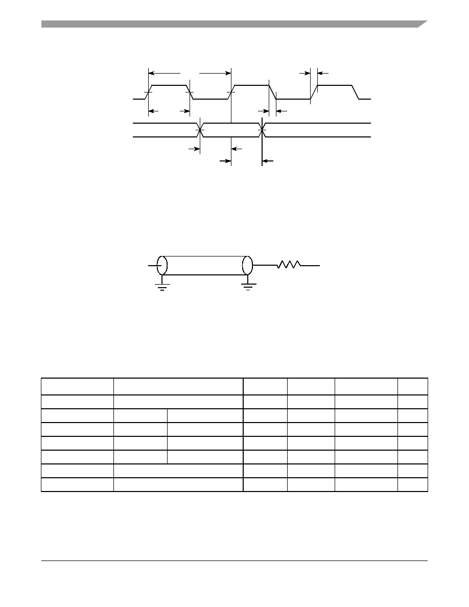
This figure shows the RMII receive AC timing diagram.
Figure 14. RMII Receive AC Timing Diagram
8.3
Management Interface Electrical Characteristics
The electrical characteristics specified here apply to MII management interface signals MDIO
(management data input/output) and MDC (management data clock).
This figure provides the AC test load for eTSEC.
Figure 15. eTSEC AC Test Load
8.3.1
MII Management DC Electrical Characteristics
The MDC and MDIO are defined to operate at a supply voltage of 2.5 V or 3.3 V. The DC electrical
Table 31. MII Management DC Electrical Characteristics When Powered at 2.5 V
Parameter
Conditions
Symbol
Min
Max
Unit
Supply voltage (2.5 V)
—
LVDD1
2.37
2.63
V
Output high voltage
IOH = –1.0 mA
LVDD1 = Min
VOH
2.00
LVDD1 + 0.3
V
Output low voltage
IOL = 1.0 mA
LVDD1 = Min
GND – 0.3
0.40
V
Input high voltage
—
LVDD1 = Min
VIH
1.7
—
V
Input low voltage
—
LVDD1 = Min
VIL
–0.3
0.70
V
Input high current
VIN = LVDD1
IIH
—20
μA
Input low current
VIN = LVDD1
IIL
–15
—
μA
REF_CLK
RXD[1:0]
tRMRDX
tRMR
tRMRH
tRMRR
tRMRF
CRS_DV
RX_ER
tRMRDV
Valid Data
Output
Z0 = 50 Ω
LVDD/2
RL = 50 Ω
相關(guān)PDF資料 |
PDF描述 |
|---|---|
| IDT709349L6PF | IC SRAM 72KBIT 6NS 100TQFP |
| IDT709159L7PFI | IC SRAM 72KBIT 7NS 100TQFP |
| MC68EN360ZQ25VL | IC MPU QUICC 32BIT 357-PBGA |
| IDT709159L6PF | IC SRAM 72KBIT 6NS 100TQFP |
| IDT70V9269S15PRF8 | IC SRAM 256KBIT 15NS 128TQFP |
相關(guān)代理商/技術(shù)參數(shù) |
參數(shù)描述 |
|---|---|
| MPC8379EVRALGA | 功能描述:微處理器 - MPU 8379 PBGA ST PbFr W/ENC RoHS:否 制造商:Atmel 處理器系列:SAMA5D31 核心:ARM Cortex A5 數(shù)據(jù)總線寬度:32 bit 最大時(shí)鐘頻率:536 MHz 程序存儲(chǔ)器大小:32 KB 數(shù)據(jù) RAM 大小:128 KB 接口類型:CAN, Ethernet, LIN, SPI,TWI, UART, USB 工作電源電壓:1.8 V to 3.3 V 最大工作溫度:+ 85 C 安裝風(fēng)格:SMD/SMT 封裝 / 箱體:FBGA-324 |
| MPC8379EVRANDA | 制造商:FREESCALE 制造商全稱:Freescale Semiconductor, Inc 功能描述:PowerQUICC? II Pro Processor Hardware Specifications |
| MPC8379EVRANFA | 制造商:FREESCALE 制造商全稱:Freescale Semiconductor, Inc 功能描述:PowerQUICC? II Pro Processor Hardware Specifications |
| MPC8379EVRANG | 功能描述:微處理器 - MPU 837X Encyrpted RoHS:否 制造商:Atmel 處理器系列:SAMA5D31 核心:ARM Cortex A5 數(shù)據(jù)總線寬度:32 bit 最大時(shí)鐘頻率:536 MHz 程序存儲(chǔ)器大小:32 KB 數(shù)據(jù) RAM 大小:128 KB 接口類型:CAN, Ethernet, LIN, SPI,TWI, UART, USB 工作電源電壓:1.8 V to 3.3 V 最大工作溫度:+ 85 C 安裝風(fēng)格:SMD/SMT 封裝 / 箱體:FBGA-324 |
| MPC8379EVRANGA | 功能描述:微處理器 - MPU 8379 PBGA ST PbFr W/ENC RoHS:否 制造商:Atmel 處理器系列:SAMA5D31 核心:ARM Cortex A5 數(shù)據(jù)總線寬度:32 bit 最大時(shí)鐘頻率:536 MHz 程序存儲(chǔ)器大小:32 KB 數(shù)據(jù) RAM 大小:128 KB 接口類型:CAN, Ethernet, LIN, SPI,TWI, UART, USB 工作電源電壓:1.8 V to 3.3 V 最大工作溫度:+ 85 C 安裝風(fēng)格:SMD/SMT 封裝 / 箱體:FBGA-324 |
發(fā)布緊急采購(gòu),3分鐘左右您將得到回復(fù)。