- 您現(xiàn)在的位置:買賣IC網 > PDF目錄45361 > MPC8343ZQADDB (FREESCALE SEMICONDUCTOR INC) 32-BIT, 266 MHz, MICROPROCESSOR, PBGA620 PDF資料下載
參數(shù)資料
| 型號: | MPC8343ZQADDB |
| 廠商: | FREESCALE SEMICONDUCTOR INC |
| 元件分類: | 微控制器/微處理器 |
| 英文描述: | 32-BIT, 266 MHz, MICROPROCESSOR, PBGA620 |
| 封裝: | 29 X 29 MM, 2.46 MM HEIGHT, 1 MM PITCH, PLASTIC, BGA-620 |
| 文件頁數(shù): | 4/79頁 |
| 文件大小: | 992K |
| 代理商: | MPC8343ZQADDB |
第1頁第2頁第3頁當前第4頁第5頁第6頁第7頁第8頁第9頁第10頁第11頁第12頁第13頁第14頁第15頁第16頁第17頁第18頁第19頁第20頁第21頁第22頁第23頁第24頁第25頁第26頁第27頁第28頁第29頁第30頁第31頁第32頁第33頁第34頁第35頁第36頁第37頁第38頁第39頁第40頁第41頁第42頁第43頁第44頁第45頁第46頁第47頁第48頁第49頁第50頁第51頁第52頁第53頁第54頁第55頁第56頁第57頁第58頁第59頁第60頁第61頁第62頁第63頁第64頁第65頁第66頁第67頁第68頁第69頁第70頁第71頁第72頁第73頁第74頁第75頁第76頁第77頁第78頁第79頁
MPC8343EA PowerQUICC II Pro Integrated Host Processor Hardware Specifications, Rev. 10
12
Freescale Semiconductor
RESET Initialization
4.3
TSEC Gigabit Reference Clock Timing
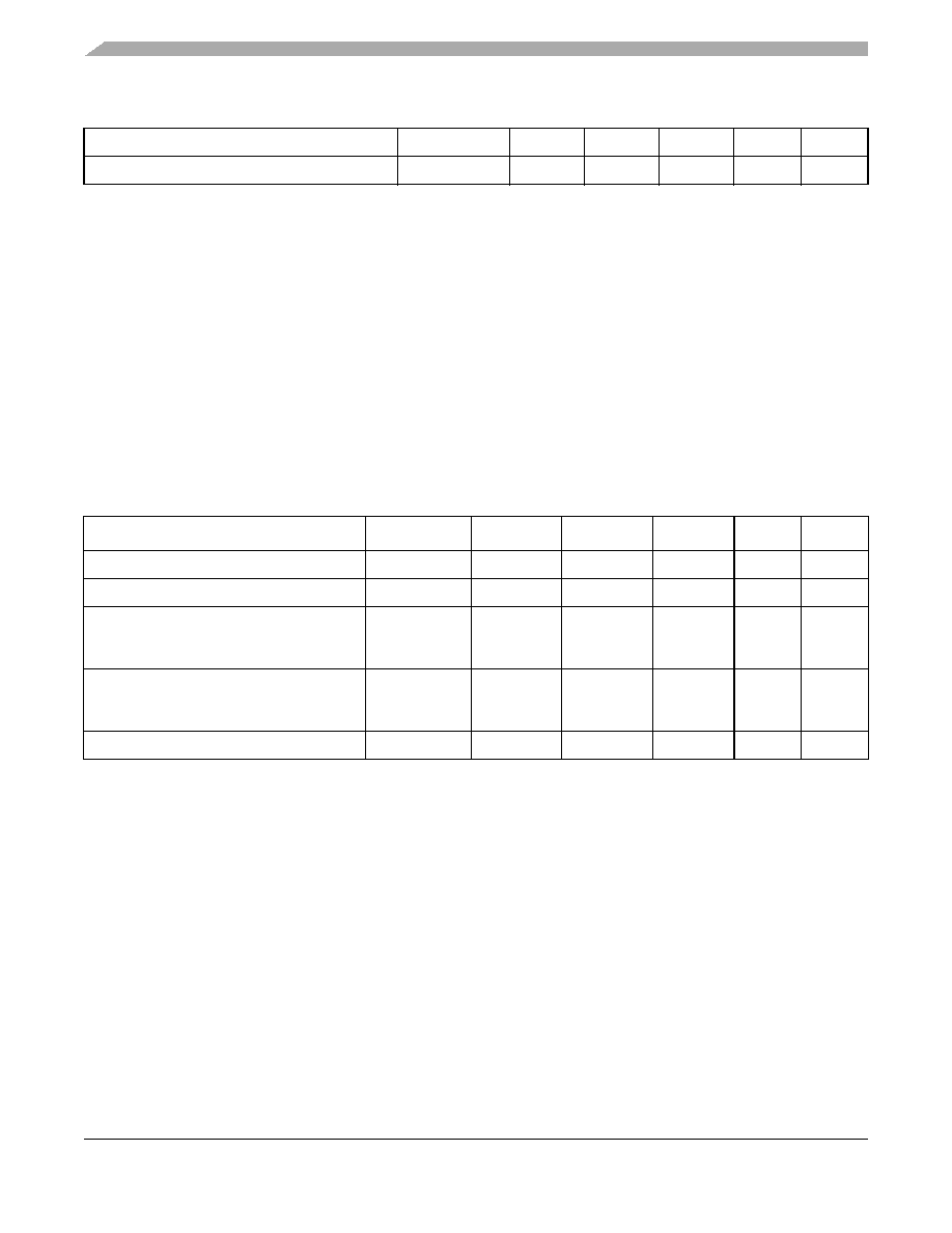
Table 8 provides the TSEC gigabit reference clocks (EC_GTX_CLK125) AC timing specifications.
5
RESET Initialization
This section describes the DC and AC electrical specifications for the reset initialization timing and
electrical requirements of the MPC8343EA.
CLKIN/PCI_CLK duty cycle
tKHK/tCLKIN
40
—
60
%
3
CLKIN/PCI_CLK jitter
—
±150
ps
4, 5
Notes:
1. Caution: The system, core, USB, security, and TSEC must not exceed their respective maximum or minimum operating
frequencies.
2. Rise and fall times for CLKIN/PCI_CLK are measured at 0.4 and 2.7 V.
3. Timing is guaranteed by design and characterization.
4. This represents the total input jitter—short term and long term—and is guaranteed by design.
5. The CLKIN/PCI_CLK driver’s closed loop jitter bandwidth should be < 500 kHz at –20 dB. The bandwidth must be set low to
allow cascade-connected PLL-based devices to track CLKIN drivers with the specified jitter.
6. Spread spectrum clocking is allowed with 1% input frequency down-spread at maximum 50 KHz modulation rate regardless
of input frequency.
Table 8. EC_GTX_CLK125 AC Timing Specifications
At recommended operating conditions with LVDD = 2.5 ± 0.125 mV/ 3.3 V ± 165 mV
Parameter
Symbol
Min
Typical
Max
Unit
Notes
EC_GTX_CLK125 frequency
tG125
—125
—
MHz
—
EC_GTX_CLK125 cycle time
tG125
—8
—
ns
—
EC_GTX_CLK rise and fall time
LVDD = 2.5 V
LVDD = 3.3 V
tG125R/tG125F
——
0.75
1.0
ns
1
EC_GTX_CLK125 duty cycle
GMII, TBI
1000Base-T for RGMII, RTBI
tG125H/tG125
45
47
—
55
53
%2
EC_GTX_CLK125 jitter
—
±150
ps
2
Notes:
1. Rise and fall times for EC_GTX_CLK125 are measured from 0.5 and 2.0 V for LVDD = 2.5 V and from 0.6 and 2.7 V for
LVDD =3.3 V.
2. EC_GTX_CLK125 is used to generate the GTX clock for the eTSEC transmitter with 2% degradation. The EC_GTX_CLK125
duty cycle can be loosened from 47%/53% as long as the PHY device can tolerate the duty cycle generated by the eTSEC
GTX_CLK. See Section 8.2.2, “RGMII and RTBI AC Timing Specifications for the duty cycle for 10Base-T and 100Base-T
reference clock.
Table 7. CLKIN AC
Timing Specifications (continued)
相關PDF資料 |
PDF描述 |
|---|---|
| MPC8343VRAGDB | 32-BIT, 400 MHz, MICROPROCESSOR, PBGA620 |
| MPC8343EVRAGDB | 32-BIT, 400 MHz, MICROPROCESSOR, PBGA620 |
| MPC8347CVRAGDA | 32-BIT, 400 MHz, MICROPROCESSOR, PBGA620 |
| MPC8347ZQADDA | 32-BIT, 266 MHz, MICROPROCESSOR, PBGA620 |
| MPC8347CZQADDA | 32-BIT, 266 MHz, MICROPROCESSOR, PBGA620 |
相關代理商/技術參數(shù) |
參數(shù)描述 |
|---|---|
| MPC8343ZQAGD | 功能描述:IC MPU PWRQUICC II PRO 620-PBGA RoHS:否 類別:集成電路 (IC) >> 嵌入式 - 微處理器 系列:MPC83xx 標準包裝:1 系列:MPC85xx 處理器類型:32-位 MPC85xx PowerQUICC III 特點:- 速度:1.2GHz 電壓:1.1V 安裝類型:表面貼裝 封裝/外殼:783-BBGA,F(xiàn)CBGA 供應商設備封裝:783-FCPBGA(29x29) 包裝:托盤 |
| MPC8343ZQAGDB | 功能描述:微處理器 - MPU 8347 PBGA PB W/O ENC RoHS:否 制造商:Atmel 處理器系列:SAMA5D31 核心:ARM Cortex A5 數(shù)據(jù)總線寬度:32 bit 最大時鐘頻率:536 MHz 程序存儲器大小:32 KB 數(shù)據(jù) RAM 大小:128 KB 接口類型:CAN, Ethernet, LIN, SPI,TWI, UART, USB 工作電源電壓:1.8 V to 3.3 V 最大工作溫度:+ 85 C 安裝風格:SMD/SMT 封裝 / 箱體:FBGA-324 |
| MPC8347 | 制造商:FREESCALE 制造商全稱:Freescale Semiconductor, Inc 功能描述:Integrated Host Processor Hardware Specifications |
| MPC8347A | 制造商:FREESCALE 制造商全稱:Freescale Semiconductor, Inc 功能描述:Integrated Host Processor Hardware Specifications |
| MPC8347CVRADDB | 功能描述:微處理器 - MPU 8347 PBGA NO-PB W/O ENC RoHS:否 制造商:Atmel 處理器系列:SAMA5D31 核心:ARM Cortex A5 數(shù)據(jù)總線寬度:32 bit 最大時鐘頻率:536 MHz 程序存儲器大小:32 KB 數(shù)據(jù) RAM 大小:128 KB 接口類型:CAN, Ethernet, LIN, SPI,TWI, UART, USB 工作電源電壓:1.8 V to 3.3 V 最大工作溫度:+ 85 C 安裝風格:SMD/SMT 封裝 / 箱體:FBGA-324 |
發(fā)布緊急采購,3分鐘左右您將得到回復。