- 您現(xiàn)在的位置:買賣IC網(wǎng) > PDF目錄4098 > MPC8314VRAGDA (Freescale Semiconductor)MPU POWERQUICC II PRO 620-PBGA PDF資料下載
參數(shù)資料
| 型號(hào): | MPC8314VRAGDA |
| 廠商: | Freescale Semiconductor |
| 文件頁(yè)數(shù): | 10/101頁(yè) |
| 文件大小: | 0K |
| 描述: | MPU POWERQUICC II PRO 620-PBGA |
| 標(biāo)準(zhǔn)包裝: | 36 |
| 系列: | MPC83xx |
| 處理器類型: | 32-位 MPC83xx PowerQUICC II Pro |
| 速度: | 400MHz |
| 電壓: | 1V |
| 安裝類型: | 表面貼裝 |
| 封裝/外殼: | 620-BBGA 裸露焊盤 |
| 供應(yīng)商設(shè)備封裝: | 620-PBGA(29x29) |
| 包裝: | 托盤 |
第1頁(yè)第2頁(yè)第3頁(yè)第4頁(yè)第5頁(yè)第6頁(yè)第7頁(yè)第8頁(yè)第9頁(yè)當(dāng)前第10頁(yè)第11頁(yè)第12頁(yè)第13頁(yè)第14頁(yè)第15頁(yè)第16頁(yè)第17頁(yè)第18頁(yè)第19頁(yè)第20頁(yè)第21頁(yè)第22頁(yè)第23頁(yè)第24頁(yè)第25頁(yè)第26頁(yè)第27頁(yè)第28頁(yè)第29頁(yè)第30頁(yè)第31頁(yè)第32頁(yè)第33頁(yè)第34頁(yè)第35頁(yè)第36頁(yè)第37頁(yè)第38頁(yè)第39頁(yè)第40頁(yè)第41頁(yè)第42頁(yè)第43頁(yè)第44頁(yè)第45頁(yè)第46頁(yè)第47頁(yè)第48頁(yè)第49頁(yè)第50頁(yè)第51頁(yè)第52頁(yè)第53頁(yè)第54頁(yè)第55頁(yè)第56頁(yè)第57頁(yè)第58頁(yè)第59頁(yè)第60頁(yè)第61頁(yè)第62頁(yè)第63頁(yè)第64頁(yè)第65頁(yè)第66頁(yè)第67頁(yè)第68頁(yè)第69頁(yè)第70頁(yè)第71頁(yè)第72頁(yè)第73頁(yè)第74頁(yè)第75頁(yè)第76頁(yè)第77頁(yè)第78頁(yè)第79頁(yè)第80頁(yè)第81頁(yè)第82頁(yè)第83頁(yè)第84頁(yè)第85頁(yè)第86頁(yè)第87頁(yè)第88頁(yè)第89頁(yè)第90頁(yè)第91頁(yè)第92頁(yè)第93頁(yè)第94頁(yè)第95頁(yè)第96頁(yè)第97頁(yè)第98頁(yè)第99頁(yè)第100頁(yè)第101頁(yè)
MPC8314E PowerQUICC II Pro Processor Hardware Specifications, Rev. 2
16
Freescale Semiconductor
DDR and DDR2 SDRAM
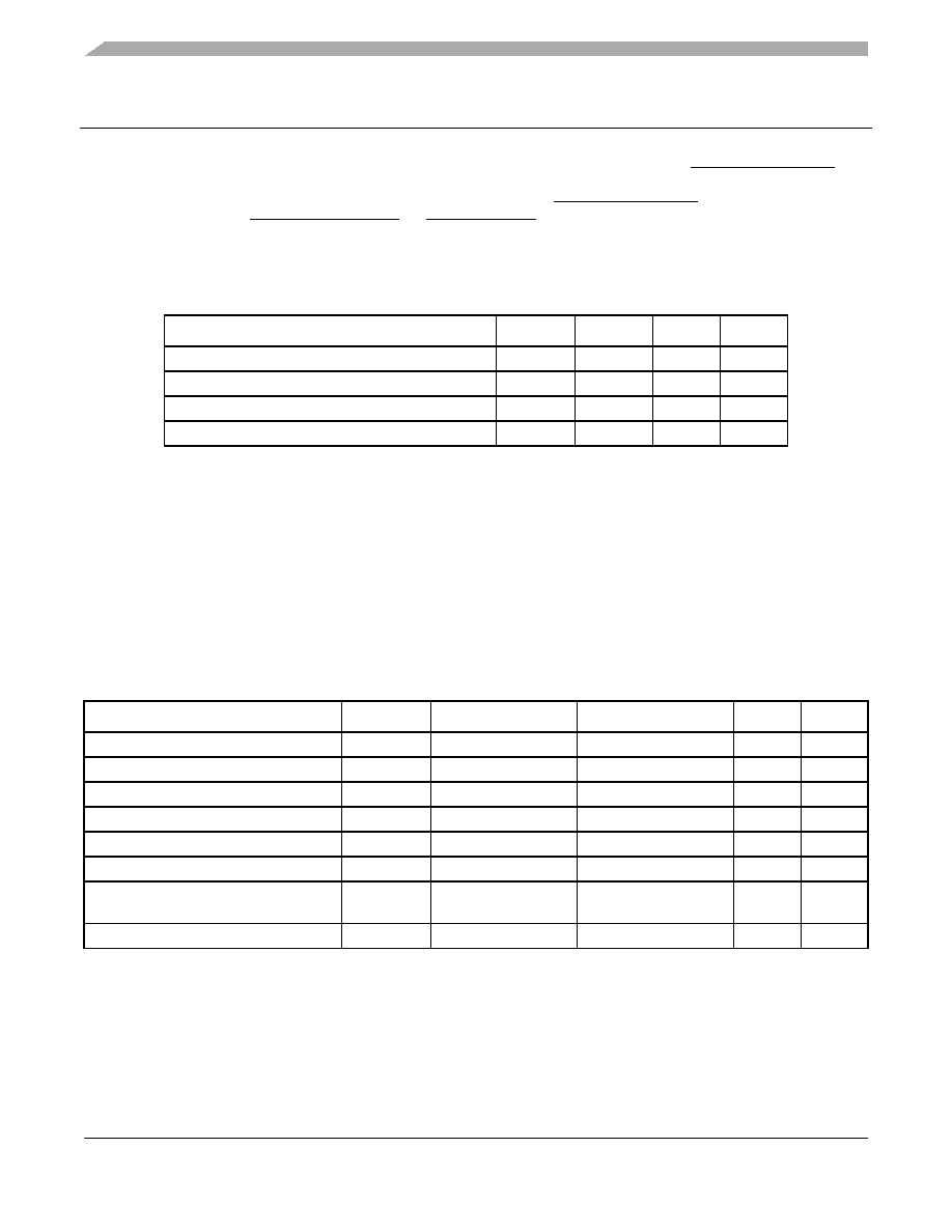
This table provides the PLL lock times.
7
DDR and DDR2 SDRAM
This section describes the DC and AC electrical specifications for the DDR SDRAM interface of the
MPC8314E. Note that DDR SDRAM is GVDD(typ) = 2.5 V and DDR2 SDRAM is GVDD(typ) = 1.8 V.
7.1 DDR and DDR2 SDRAM DC Electrical Characteristics
This table provides the recommended operating conditions for the DDR2 SDRAM component(s) of the
MPC8314E when GVDD(typ) = 1.8 V.
Note:
1. tPCI_SYNC_IN is the clock period of the input clock applied to PCI_SYNC_IN. When the device is In PCI host mode the primary
clock is applied to the SYS_CLK_IN input, and PCI_SYNC_IN period depends on the value of CFG_SYS_CLKIN_DIV.
2. tSYS_CLK_IN is the clock period of the input clock applied to SYS_CLK_IN. It is only valid when the device is in PCI host mode.
3. POR configuration signals consists of CFG_RESET_SOURCE[0:3] and CFG_SYS_CLKIN_DIV.
4. The parameter names CFG_SYS_CLKIN_DIV and CFG_CLKIN_DIV are used interchangeably in this document.
Table 10. PLL Lock Times
Parameter/Condition
Min
Max
Unit
Note
System PLL lock times
—
100
s—
e300 core PLL lock times
—
100
s—
SerDes (SGMII/PCI Exp Phy) PLL lock times
—
100
s—
USB phy PLL lock times
—
100
s—
Table 11. DDR2 SDRAM DC Electrical Characteristics for GVDD(typ) = 1.8 V
Parameter/Condition
Symbol
Min
Max
Unit
Note
I/O supply voltage
GVDD
1.7
1.9
V
1
I/O reference voltage
MVREF
0.49
GVDD
0.51
GVDD
V
2
I/O termination voltage
VTT
MVREF – 0.04
MVREF + 0.04
V
3
Input high voltage
VIH
MVREF+ 0.125
GVDD + 0.3
V
—
Input low voltage
VIL
–0.3
MVREF – 0.125
V
—
Output leakage current
IOZ
–9.9
9.9
A4
Output high current (VOUT = 1.420 V,
GVDD= 1.7V)
IOH
–13.4
—
mA
—
Output low current (VOUT = 0.280 V)
IOL
13.4
—
mA
Note:
1. GVDD is expected to be within 50 mV of the DRAM GVDD at all times.
2. MVREF is expected to be equal to 0.5
GVDD, and to track GVDD DC variations as measured at the receiver. Peak-to-peak
noise on MVREF may not exceed ±2% of the DC value.
3. VTT is not applied directly to the device. It is the supply to which far end signal termination is made and is expected to be
equal to MVREF. This rail should track variations in the DC level of MVREF.
4. Output leakage is measured with all outputs disabled, 0 V
V
OUT GVDD.
Table 9. RESET Initialization Timing Specifications (continued)
相關(guān)PDF資料 |
PDF描述 |
|---|---|
| GMC28DTES | CONN EDGECARD 56POS .100 EYELET |
| IDT7143SA20PF8 | IC SRAM 32KBIT 20NS 100TQFP |
| AMM43DRST-S288 | CONN EDGECARD 86POS .156 EXTEND |
| IDT7133SA20PF8 | IC SRAM 32KBIT 20NS 100TQFP |
| HMC65DRYN-S13 | CONN EDGECARD 130PS .100 EXTEND |
相關(guān)代理商/技術(shù)參數(shù) |
參數(shù)描述 |
|---|---|
| MPC8315 | 制造商:FREESCALE 制造商全稱:Freescale Semiconductor, Inc 功能描述:MPC8315E PowerQUICC II Pro Processor Hardware Specifications |
| MPC8315CVRADDA | 功能描述:微處理器 - MPU NON-ENCRYPT RoHS:否 制造商:Atmel 處理器系列:SAMA5D31 核心:ARM Cortex A5 數(shù)據(jù)總線寬度:32 bit 最大時(shí)鐘頻率:536 MHz 程序存儲(chǔ)器大小:32 KB 數(shù)據(jù) RAM 大小:128 KB 接口類型:CAN, Ethernet, LIN, SPI,TWI, UART, USB 工作電源電壓:1.8 V to 3.3 V 最大工作溫度:+ 85 C 安裝風(fēng)格:SMD/SMT 封裝 / 箱體:FBGA-324 |
| MPC8315CVRAFDA | 功能描述:微處理器 - MPU NON-ENCRYPT RoHS:否 制造商:Atmel 處理器系列:SAMA5D31 核心:ARM Cortex A5 數(shù)據(jù)總線寬度:32 bit 最大時(shí)鐘頻率:536 MHz 程序存儲(chǔ)器大小:32 KB 數(shù)據(jù) RAM 大小:128 KB 接口類型:CAN, Ethernet, LIN, SPI,TWI, UART, USB 工作電源電壓:1.8 V to 3.3 V 最大工作溫度:+ 85 C 安裝風(fēng)格:SMD/SMT 封裝 / 箱體:FBGA-324 |
| MPC8315CVRAGDA | 功能描述:微處理器 - MPU NON-ENCRYPT RoHS:否 制造商:Atmel 處理器系列:SAMA5D31 核心:ARM Cortex A5 數(shù)據(jù)總線寬度:32 bit 最大時(shí)鐘頻率:536 MHz 程序存儲(chǔ)器大小:32 KB 數(shù)據(jù) RAM 大小:128 KB 接口類型:CAN, Ethernet, LIN, SPI,TWI, UART, USB 工作電源電壓:1.8 V to 3.3 V 最大工作溫度:+ 85 C 安裝風(fēng)格:SMD/SMT 封裝 / 箱體:FBGA-324 |
| MPC8315E | 制造商:FREESCALE 制造商全稱:Freescale Semiconductor, Inc 功能描述:PowerQUICC? II Pro Processor Hardware Specifications |
發(fā)布緊急采購(gòu),3分鐘左右您將得到回復(fù)。