- 您現(xiàn)在的位置:買賣IC網(wǎng) > PDF目錄3949 > MPC8313ECVRAFF (Freescale Semiconductor)IC MPU POWERQUICC II PRO 516PBGA PDF資料下載
參數(shù)資料
| 型號: | MPC8313ECVRAFF |
| 廠商: | Freescale Semiconductor |
| 文件頁數(shù): | 51/99頁 |
| 文件大?。?/td> | 0K |
| 描述: | IC MPU POWERQUICC II PRO 516PBGA |
| 標(biāo)準(zhǔn)包裝: | 40 |
| 系列: | MPC83xx |
| 處理器類型: | 32-位 MPC83xx PowerQUICC II Pro |
| 速度: | 333MHz |
| 電壓: | 0.95 V ~ 1.05 V |
| 安裝類型: | 表面貼裝 |
| 封裝/外殼: | 516-BBGA 裸露焊盤 |
| 供應(yīng)商設(shè)備封裝: | 516-PBGAPGE(27x27) |
| 包裝: | 托盤 |
| 配用: | MPC8313E-RDB-ND - BOARD PROCESSOR |
第1頁第2頁第3頁第4頁第5頁第6頁第7頁第8頁第9頁第10頁第11頁第12頁第13頁第14頁第15頁第16頁第17頁第18頁第19頁第20頁第21頁第22頁第23頁第24頁第25頁第26頁第27頁第28頁第29頁第30頁第31頁第32頁第33頁第34頁第35頁第36頁第37頁第38頁第39頁第40頁第41頁第42頁第43頁第44頁第45頁第46頁第47頁第48頁第49頁第50頁當(dāng)前第51頁第52頁第53頁第54頁第55頁第56頁第57頁第58頁第59頁第60頁第61頁第62頁第63頁第64頁第65頁第66頁第67頁第68頁第69頁第70頁第71頁第72頁第73頁第74頁第75頁第76頁第77頁第78頁第79頁第80頁第81頁第82頁第83頁第84頁第85頁第86頁第87頁第88頁第89頁第90頁第91頁第92頁第93頁第94頁第95頁第96頁第97頁第98頁第99頁
MPC8313E PowerQUICC II Pro Processor Hardware Specifications, Rev. 4
Freescale Semiconductor
55
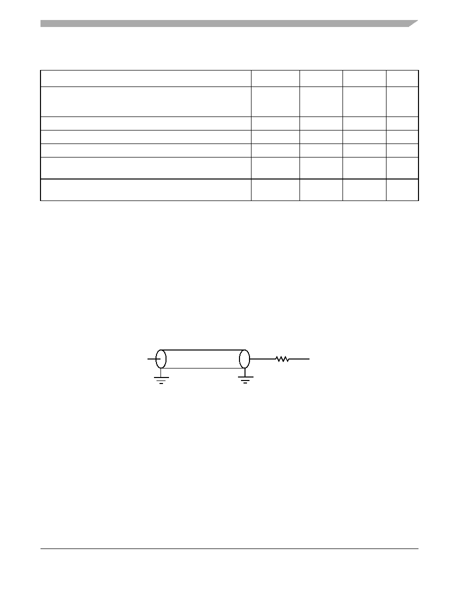
This figure provides the AC test load for the I2C.
Figure 46. I2C AC Test Load
Data hold time:
CBUS compatible masters
I2C bus devices
tI2DXKL
—
02
—
0.93
s
Fall time of both SDA and SCL signals5
tI2CF
—300
ns
Setup time for STOP condition
tI2PVKH
0.6
—
s
Bus free time between a STOP and START condition
tI2KHDX
1.3
—
s
Noise margin at the LOW level for each connected device (including
hysteresis)
VNL
0.1
NV
DD
—V
Noise margin at the HIGH level for each connected device (including
hysteresis)
VNH
0.2
NV
DD
—V
Notes:
1. The symbols used for timing specifications follow the pattern of t(first two letters of functional block)(signal)(state)(reference)(state) for
inputs and t(first two letters of functional block)(reference)(state)(signal)(state) for outputs. For example, tI2DVKH symbolizes I
2C timing
(I2) with respect to the time data input signals (D) reach the valid state (V) relative to the tI2C clock reference (K) going to
the high (H) state or setup time. Also, tI2SXKL symbolizes I
2C timing (I2) for the time that the data with respect to the start
condition (S) went invalid (X) relative to the tI2C clock reference (K) going to the low (L) state or hold time. Also, tI2PVKH
symbolizes I2C timing (I2) for the time that the data with respect to the stop condition (P) reaching the valid state (V) relative
to the tI2C clock reference (K) going to the high (H) state or setup time. For rise and fall times, the latter convention is used
with the appropriate letter: R (rise) or F (fall).
2. The MPC8313E provides a hold time of at least 300 ns for the SDA signal (referred to the VIHmin of the SCL signal) to bridge
the undefined region of the falling edge of SCL.
3. The maximum tI2DVKH has only to be met if the device does not stretch the LOW period (tI2CL) of the SCL signal.
4. CB = capacitance of one bus line in pF.
5. The MPC8313E does not follow the I2C-BUS Specifications, Version 2.1, regarding the tI2CF AC parameter.
Table 49. I2C AC Electrical Specifications (continued)
All values refer to VIH (min) and VIL (max) levels (see Table 48).
Parameter
Symbol1
Min
Max
Unit
Output
Z0 = 50
NVDD/2
RL = 50
相關(guān)PDF資料 |
PDF描述 |
|---|---|
| 84533-7 | CONN FFC 7POS 1.25MM R/A PCB |
| 1-84533-5 | CONN FFC 15POS 1.25MM RT ANG |
| 487925-8 | CONN FFC VERT 11POS 2.54MM ZIF |
| 487576-3 | CONN ZIF LINE 11POS VERT |
| 1734798-7 | CONN HOUSING FPC 7POS R/A SMD |
相關(guān)代理商/技術(shù)參數(shù) |
參數(shù)描述 |
|---|---|
| MPC8313ECVRAFFA | 制造商:FREESCALE 制造商全稱:Freescale Semiconductor, Inc 功能描述:PowerQUICC? II Pro Processor Hardware Specifications |
| MPC8313ECVRAFFB | 功能描述:微處理器 - MPU PBGA W/ ENCR RoHS:否 制造商:Atmel 處理器系列:SAMA5D31 核心:ARM Cortex A5 數(shù)據(jù)總線寬度:32 bit 最大時鐘頻率:536 MHz 程序存儲器大小:32 KB 數(shù)據(jù) RAM 大小:128 KB 接口類型:CAN, Ethernet, LIN, SPI,TWI, UART, USB 工作電源電壓:1.8 V to 3.3 V 最大工作溫度:+ 85 C 安裝風(fēng)格:SMD/SMT 封裝 / 箱體:FBGA-324 |
| MPC8313ECVRAFFC | 功能描述:微處理器 - MPU 8313 REV2.2 W/ENC EXT RoHS:否 制造商:Atmel 處理器系列:SAMA5D31 核心:ARM Cortex A5 數(shù)據(jù)總線寬度:32 bit 最大時鐘頻率:536 MHz 程序存儲器大小:32 KB 數(shù)據(jù) RAM 大小:128 KB 接口類型:CAN, Ethernet, LIN, SPI,TWI, UART, USB 工作電源電壓:1.8 V to 3.3 V 最大工作溫度:+ 85 C 安裝風(fēng)格:SMD/SMT 封裝 / 箱體:FBGA-324 |
| MPC8313ECVRAGDB | 功能描述:微處理器 - MPU PBGA W/ ENCR RoHS:否 制造商:Atmel 處理器系列:SAMA5D31 核心:ARM Cortex A5 數(shù)據(jù)總線寬度:32 bit 最大時鐘頻率:536 MHz 程序存儲器大小:32 KB 數(shù)據(jù) RAM 大小:128 KB 接口類型:CAN, Ethernet, LIN, SPI,TWI, UART, USB 工作電源電壓:1.8 V to 3.3 V 最大工作溫度:+ 85 C 安裝風(fēng)格:SMD/SMT 封裝 / 箱體:FBGA-324 |
| MPC8313ECVRAGDC | 功能描述:微處理器 - MPU 8313 REV2.2 W/ENC EXT RoHS:否 制造商:Atmel 處理器系列:SAMA5D31 核心:ARM Cortex A5 數(shù)據(jù)總線寬度:32 bit 最大時鐘頻率:536 MHz 程序存儲器大小:32 KB 數(shù)據(jù) RAM 大小:128 KB 接口類型:CAN, Ethernet, LIN, SPI,TWI, UART, USB 工作電源電壓:1.8 V to 3.3 V 最大工作溫度:+ 85 C 安裝風(fēng)格:SMD/SMT 封裝 / 箱體:FBGA-324 |
發(fā)布緊急采購,3分鐘左右您將得到回復(fù)。