- 您現(xiàn)在的位置:買(mǎi)賣(mài)IC網(wǎng) > PDF目錄45354 > MPC8245ARZU400D (MOTOROLA INC) 32-BIT, 400 MHz, RISC PROCESSOR, PBGA352 PDF資料下載
參數(shù)資料
| 型號(hào): | MPC8245ARZU400D |
| 廠商: | MOTOROLA INC |
| 元件分類(lèi): | 微控制器/微處理器 |
| 英文描述: | 32-BIT, 400 MHz, RISC PROCESSOR, PBGA352 |
| 封裝: | TBGA-352 |
| 文件頁(yè)數(shù): | 10/12頁(yè) |
| 文件大小: | 152K |
| 代理商: | MPC8245ARZU400D |
MOTOROLA MPC8245 Part Number Specification for the MPC8245ARZUnnnX Series
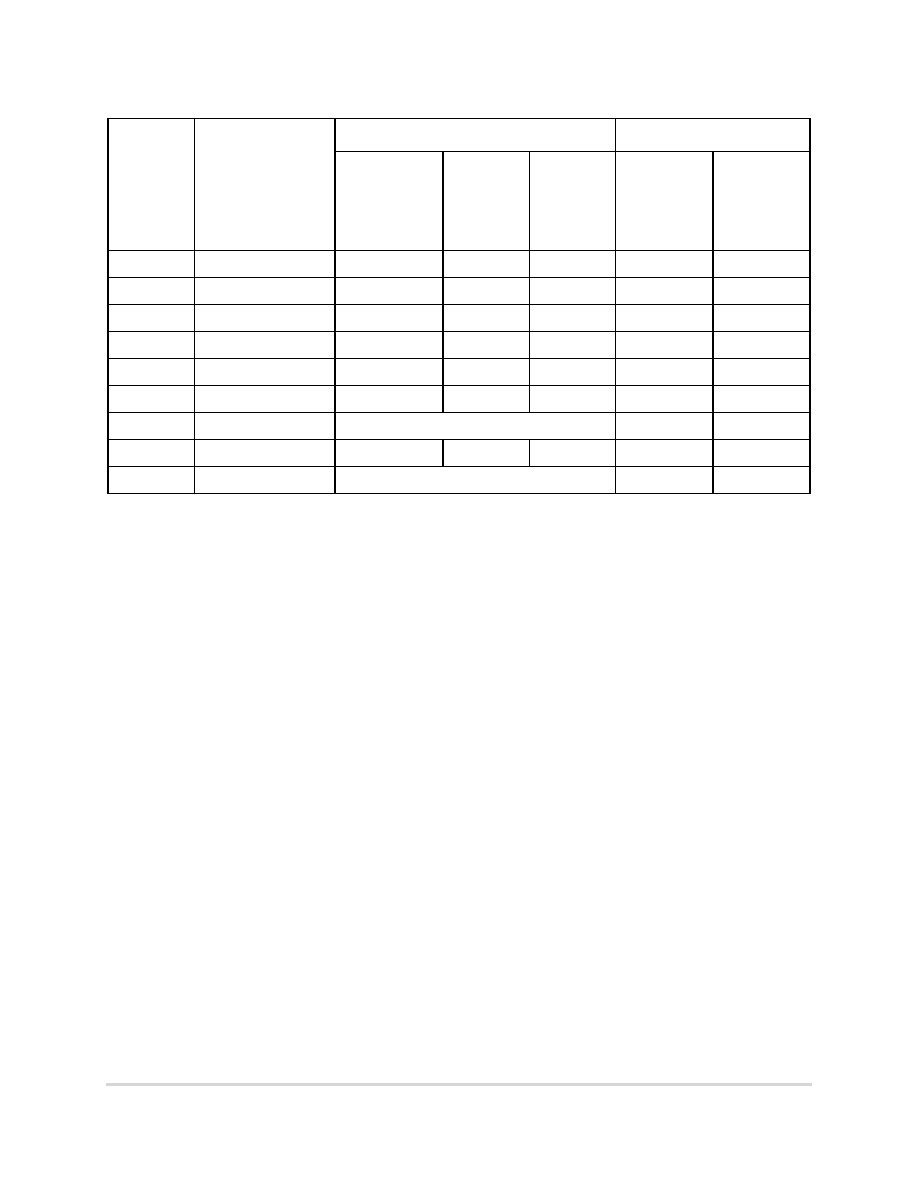
7
PLL Configuration
18
11000
273–535
68–132
204–396
2.5 (2)
3 (2)
19
11001
366–661
72–132
180–330
2 (2)
2.5 (2)
1A
11010
509–661
50–66
200–264
1 (4)
4 (2)
1B
1101113
343–661
68–132
204–396
2 (2)
3 (2)
1C
11100
446–661
66–99
198–297
1.5 (2)
3 (2)
1D
11101
486–661
72–99
180–248
1.5 (2)
2.5(2)
1E (Rev. B)
1111010
Not usable
Off
1E (Rev. D)
11110
333–575
66–114
231–399
2(2)
3.5(2)
1F
1111110
Not usable
Off
Notes:
1. Limited by maximum PCI input frequency (66 MHz).
2. Limited by maximum system memory interface operating frequency (133 MHz).
3. Limited by minimum memory VCO frequency (132 MHz).
4. Limited due to maximum memory VCO frequency (372 MHz).
5. Limited by maximum CPU operating frequency (400 MHz).
6. Limited by minimum CPU VCO frequency (360 MHz).
7. Limited by maximum CPU VCO frequency (800 MHz).
8. Limited by minimum CPU operating frequency (100 MHz).
9. Limited by minimum memory bus frequency (50 MHz).
10.In clock off mode, no clocking occurs inside the MPC8245 regardless of the PCI_SYNC_IN input.
11.Range values are shown rounded down to the nearest whole number (decimal place accuracy removed) for clarity.
12.PLL_CFG[0:4] settings not listed are reserved.
13.Multiplier ratios for this PLL_CFG[0:4] setting are different from the MPC8240 and are not backwards-compatible.
14.PCI_SYNC_IN range for this PLL_CFG[0:4] setting is different from the MPC8240 and may not be fully
backwards-compatible.
15.Bits 7– 4 of register offset <0xE2> contain the PLL_CFG[0:4] setting value.
16.In PLL bypass mode, the PCI_SYNC_IN input signal clocks the internal processor directly, the peripheral logic PLL
is disabled, and the bus mode is set for 1:1 (PCI:Mem) mode operation. This mode is intended for hardware
modeling support. The AC timing specifications given in this document do not apply in the PLL bypass mode.
17.In dual PLL bypass mode, the PCI_SYNC_IN input signal clocks the internal peripheral logic directly, the peripheral
logic PLL is disabled, and the bus mode is set for 1:1 (PCI_SYNC_IN:Mem) mode operation. In this mode, the
OSC_IN input signal clocks the internal processor directly in 1:1 (OSC_IN:CPU) mode operation, and the
processor PLL is disabled. The PCI_SYNC_IN and OSC_IN input clocks must be externally synchronized. This
mode is intended for hardware modeling support. The AC timing specifications given in this document do not apply
in the dual PLL bypass mode.
Table 17. PLL Configurations for the 400-MHz Part Offering (continued)
Ref
PLL_CFG[0:4]11,14,15
400-MHz Part 9
Multipliers
PCI Clock Input
(PCI_SYNC_IN)
Range 1
(MHz)
Periph
Logic/Mem
Bus Clock
Range
(MHz)
CPU Clock
Range
(MHz)
PCI-to-Mem
(Mem VCO)
Mem-to-CPU
(CPU VCO)
相關(guān)PDF資料 |
PDF描述 |
|---|---|
| MPC8245ARZU466D | 32-BIT, 466 MHz, MICROPROCESSOR, PBGA352 |
| MPC8245LVV333D | 32-BIT, 333 MHz, RISC PROCESSOR, PBGA352 |
| MPC8245LVV350D | 32-BIT, 350 MHz, RISC PROCESSOR, PBGA352 |
| MPC8245LZU266D | 32-BIT, 266 MHz, RISC PROCESSOR, PBGA352 |
| MPC8245LVV300D | 32-BIT, 300 MHz, RISC PROCESSOR, PBGA352 |
相關(guān)代理商/技術(shù)參數(shù) |
參數(shù)描述 |
|---|---|
| MPC8245ARZU400D | 制造商:Freescale Semiconductor 功能描述:IC 32BIT MPU 400MHZ BGA-352 |
| MPC8245ARZU466D | 制造商:FREESCALE 制造商全稱(chēng):Freescale Semiconductor, Inc 功能描述:Part Number Specification for the MPC8245ARZUnnnX Series |
| MPC8245EC | 制造商:FREESCALE 制造商全稱(chēng):Freescale Semiconductor, Inc 功能描述:MPC8245 Integrated Processor Hardware Specifications |
| MPC8245ECS02AD | 制造商:FREESCALE 制造商全稱(chēng):Freescale Semiconductor, Inc 功能描述:MPC8245 Integrated Processor Hardware Specifications |
| MPC8245LVV266D | 功能描述:微處理器 - MPU 266MHz 505.4MIPS RoHS:否 制造商:Atmel 處理器系列:SAMA5D31 核心:ARM Cortex A5 數(shù)據(jù)總線寬度:32 bit 最大時(shí)鐘頻率:536 MHz 程序存儲(chǔ)器大小:32 KB 數(shù)據(jù) RAM 大小:128 KB 接口類(lèi)型:CAN, Ethernet, LIN, SPI,TWI, UART, USB 工作電源電壓:1.8 V to 3.3 V 最大工作溫度:+ 85 C 安裝風(fēng)格:SMD/SMT 封裝 / 箱體:FBGA-324 |
發(fā)布緊急采購(gòu),3分鐘左右您將得到回復(fù)。