- 您現(xiàn)在的位置:買賣IC網(wǎng) > PDF目錄45342 > MPC5607BMLQ4R (FREESCALE SEMICONDUCTOR INC) FLASH, 48 MHz, MICROCONTROLLER, PQFP144 PDF資料下載
參數(shù)資料
| 型號(hào): | MPC5607BMLQ4R |
| 廠商: | FREESCALE SEMICONDUCTOR INC |
| 元件分類: | 微控制器/微處理器 |
| 英文描述: | FLASH, 48 MHz, MICROCONTROLLER, PQFP144 |
| 封裝: | 20 X 20 MM, 0.50 MM PITCH, 1.40 HEIGHT, LQFP-144 |
| 文件頁(yè)數(shù): | 83/106頁(yè) |
| 文件大?。?/td> | 667K |
| 代理商: | MPC5607BMLQ4R |
第1頁(yè)第2頁(yè)第3頁(yè)第4頁(yè)第5頁(yè)第6頁(yè)第7頁(yè)第8頁(yè)第9頁(yè)第10頁(yè)第11頁(yè)第12頁(yè)第13頁(yè)第14頁(yè)第15頁(yè)第16頁(yè)第17頁(yè)第18頁(yè)第19頁(yè)第20頁(yè)第21頁(yè)第22頁(yè)第23頁(yè)第24頁(yè)第25頁(yè)第26頁(yè)第27頁(yè)第28頁(yè)第29頁(yè)第30頁(yè)第31頁(yè)第32頁(yè)第33頁(yè)第34頁(yè)第35頁(yè)第36頁(yè)第37頁(yè)第38頁(yè)第39頁(yè)第40頁(yè)第41頁(yè)第42頁(yè)第43頁(yè)第44頁(yè)第45頁(yè)第46頁(yè)第47頁(yè)第48頁(yè)第49頁(yè)第50頁(yè)第51頁(yè)第52頁(yè)第53頁(yè)第54頁(yè)第55頁(yè)第56頁(yè)第57頁(yè)第58頁(yè)第59頁(yè)第60頁(yè)第61頁(yè)第62頁(yè)第63頁(yè)第64頁(yè)第65頁(yè)第66頁(yè)第67頁(yè)第68頁(yè)第69頁(yè)第70頁(yè)第71頁(yè)第72頁(yè)第73頁(yè)第74頁(yè)第75頁(yè)第76頁(yè)第77頁(yè)第78頁(yè)第79頁(yè)第80頁(yè)第81頁(yè)第82頁(yè)當(dāng)前第83頁(yè)第84頁(yè)第85頁(yè)第86頁(yè)第87頁(yè)第88頁(yè)第89頁(yè)第90頁(yè)第91頁(yè)第92頁(yè)第93頁(yè)第94頁(yè)第95頁(yè)第96頁(yè)第97頁(yè)第98頁(yè)第99頁(yè)第100頁(yè)第101頁(yè)第102頁(yè)第103頁(yè)第104頁(yè)第105頁(yè)第106頁(yè)
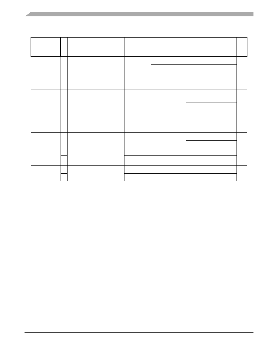
MPC5607B Microcontroller Data Sheet, Rev. 5
Electrical characteristics
Freescale Semiconductor
78
IINJ
SR — Input current Injection
Current
injection on
one ADC_1
input, different
from the
converted one
VDD = 3.3 V ± 10%
–5
—
5
mA
VDD = 5.0 V ± 10%
–5
—
5
INLP
CC T Absolute Integral
non-linearity-Precise channels
No overload
—
1
3
LSB
INLX
CC T Absolute Integral
non-linearity-Extended
channels
No overload
—
1.5
5
LSB
DNL
CC T Absolute Differential
non-linearity
No overload
—
0.5
1
LSB
OFS
CC T Absolute Offset error
——
2
—
LSB
GNE
CC T Absolute Gain error
——
2
—
LSB
TUEP7
CC P Total Unadjusted Error for
precise channels, input only
pins
Without current injection
–6
—
6
LSB
T
With current injection
–8
—
8
TUEX7
CC T Total Unadjusted Error for
extended channel
Without current injection
–10
—
10
LSB
T
With current injection
–12
—
12
1 V
DD = 3.3 V ± 10% / 5.0 V ± 10%, TA = –40 to 125 °C, unless otherwise specified
2 Analog and digital V
SS must be common (to be tied together externally).
3 V
AINx may exceed VSS_ADC1 and VDD_ADC1 limits, remaining on absolute maximum ratings, but the results of the
conversion will be clamped respectively to 0x000 or 0xFFF.
4 During the sample time the input capacitance C
S can be charged/discharged by the external source. The internal
resistance of the analog source must allow the capacitance to reach its final voltage level within tADC1_S. After the end
of the sample time tADC1_S, changes of the analog input voltage have no effect on the conversion result. Values for the
sample clock tADC1_S depend on programming.
5 This parameter does not include the sample time t
ADC1_S, but only the time for determining the digital result and the
time to load the result’s register with the conversion result.
6 Duty cycle is ensured by using system clock without prescaling. When ADCLKSEL = 0, the duty cycle is ensured by
internal divider by 2.
7 Total Unadjusted Error: The maximum error that occurs without adjusting Offset and Gain errors. This error is a
combination of Offset, Gain and Integral Linearity errors.
Table 42. ADC_1 conversion characteristics (12-bit ADC_1) (continued)
Symbol
C
Parameter
Conditions1
Value
Unit
Min
Typ
Max
相關(guān)PDF資料 |
PDF描述 |
|---|---|
| MPC5607BVLU4 | FLASH, 48 MHz, MICROCONTROLLER, PQFP176 |
| MPC5607BVLL4 | FLASH, 48 MHz, MICROCONTROLLER, PQFP100 |
| MPC5607BVLQ6R | FLASH, 64 MHz, MICROCONTROLLER, PQFP144 |
| MPC5607BF0CLU6R | 32-BIT, FLASH, 64 MHz, MICROCONTROLLER, PQFP176 |
| MPC5607BF0MLU4 | 32-BIT, FLASH, 48 MHz, MICROCONTROLLER, PQFP176 |
相關(guān)代理商/技術(shù)參數(shù) |
參數(shù)描述 |
|---|---|
| MPC5607CECLLR | 制造商:FREESCALE 制造商全稱:Freescale Semiconductor, Inc 功能描述:Microcontroller |
| MPC5607CECLQR | 制造商:FREESCALE 制造商全稱:Freescale Semiconductor, Inc 功能描述:Microcontroller |
| MPC5607CECLUR | 制造商:FREESCALE 制造商全稱:Freescale Semiconductor, Inc 功能描述:Microcontroller |
| MPC5607CEMLLR | 制造商:FREESCALE 制造商全稱:Freescale Semiconductor, Inc 功能描述:Microcontroller |
| MPC5607CEMLQR | 制造商:FREESCALE 制造商全稱:Freescale Semiconductor, Inc 功能描述:Microcontroller |
發(fā)布緊急采購(gòu),3分鐘左右您將得到回復(fù)。