- 您現(xiàn)在的位置:買賣IC網(wǎng) > PDF目錄359644 > MPC5534AVZ40 (飛思卡爾半導(dǎo)體(中國)有限公司) Microcontroller PDF資料下載
參數(shù)資料
| 型號: | MPC5534AVZ40 |
| 廠商: | 飛思卡爾半導(dǎo)體(中國)有限公司 |
| 英文描述: | Microcontroller |
| 中文描述: | 微控制器 |
| 文件頁數(shù): | 30/50頁 |
| 文件大小: | 1148K |
| 代理商: | MPC5534AVZ40 |
第1頁第2頁第3頁第4頁第5頁第6頁第7頁第8頁第9頁第10頁第11頁第12頁第13頁第14頁第15頁第16頁第17頁第18頁第19頁第20頁第21頁第22頁第23頁第24頁第25頁第26頁第27頁第28頁第29頁當(dāng)前第30頁第31頁第32頁第33頁第34頁第35頁第36頁第37頁第38頁第39頁第40頁第41頁第42頁第43頁第44頁第45頁第46頁第47頁第48頁第49頁第50頁
MPC5534 Microcontroller Data Sheet, Rev. 0
Preliminary—Subject to Change Without Notice
Electrical Characteristics
Freescale Semiconductor
30
3.13.3
Nexus Timing
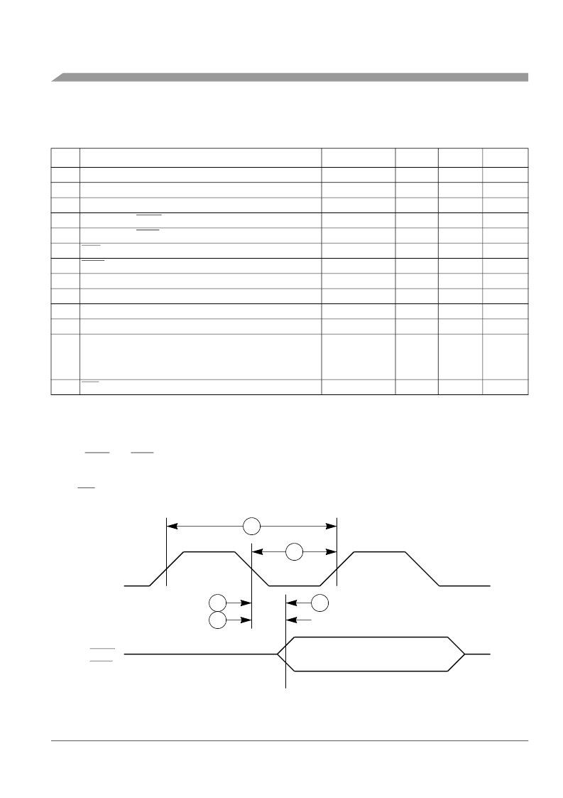
Figure 9. Nexus Output Timing
Table 21. Nexus Debug Port Timing
1
1
JTAG specifications in this table apply when used for debug functionality. All Nexus timing relative to MCKO is measured from
50% of MCKO and 50% of the respective signal. Nexus timing specified at VDD = 1.35V to 1.65V, VDDE = 2.25V to 3.6V,
VDD33 and VDDSYN = 3.0V to 3.6V, T
A
= TL to TH, and CL = 30pF with DSC = 0b10.
2
The Nexus AUX port can only run up to 82MHz. The NPC_PCR[MCKO_DIV] must be set to divide by 2 if the system frequency
is above 82MHz
3
MDO, MSEO, and EVTO data is held valid until next MCKO low cycle.
4
The maximum frequency must be limited to approximately 16 MHz (VDDE= 2.25 to 3.0 volts) or 22 MHz (VDDE= 3.0 to 3.6
volts) to meet the timing specification for t
JOV
of 0.2 x t
JCYC
as outlined in the IEEE-ISTO 5001-2003 specification.
5
The RDY pin timing is asynchronous to MCKO. The timing is guaranteed by design to function correctly.
Num
Characteristic
Symbol
Min
Max
Unit
1
MCKO Cycle Time
t
MCYC
t
MDC
t
MDOV
t
MSEOV
t
EVTOV
t
EVTIPW
t
EVTOPW
t
TCYC
t
TDC
t
NTDIS,
t
NTMSS
t
NTDIH,
t
NTMSH
t
JOV
1
2
8
t
CYC
%
2
MCKO Duty Cycle
MCKO Low to MDO Data Valid
3
MCKO Low to MSEO Data Valid
3
MCKO Low to EVTO Data Valid
3
40
60
3
–1.5
3.0
ns
4
–1.5
3.0
ns
5
–1.5
3.0
ns
6
EVTI Pulse Width
4.0
—
t
TCYC
t
MCYC
t
CYC
%
7
EVTO Pulse Width
1
4
4
8
TCK Cycle Time
—
9
TCK Duty Cycle
40
60
10
TDI, TMS Data Setup Time
8
—
ns
11
TDI, TMS Data Hold Time
5
—
ns
12
TCK Low to TDO Data Valid
VDDE = 2.25 to 3.0 volts
0
12
ns
VDDE = 3.0 to 3.6 volts
RDY Valid to MCKO
5
0
9
ns
13
—
—
—
—
1
2
3
4
5
MCKO
MDO
MSEO
EVTO
Output Data Valid
相關(guān)PDF資料 |
PDF描述 |
|---|---|
| MPC5534AVZ40R2 | Microcontroller |
| MPC5534AVZ66 | Microcontroller |
| MPC5534AVZ66R2 | Microcontroller |
| MPC5534AVZ80 | Microcontroller |
| MPC5534AVZ80R2 | Microcontroller |
相關(guān)代理商/技術(shù)參數(shù) |
參數(shù)描述 |
|---|---|
| MPC5534AVZ40R2 | 制造商:FREESCALE 制造商全稱:Freescale Semiconductor, Inc 功能描述:Microcontroller |
| MPC5534AVZ66 | 制造商:FREESCALE 制造商全稱:Freescale Semiconductor, Inc 功能描述:Microcontroller |
| MPC5534AVZ66R2 | 制造商:FREESCALE 制造商全稱:Freescale Semiconductor, Inc 功能描述:Microcontroller |
| MPC5534AVZ80 | 制造商:FREESCALE 制造商全稱:Freescale Semiconductor, Inc 功能描述:Microcontroller |
| MPC5534AVZ80R2 | 制造商:FREESCALE 制造商全稱:Freescale Semiconductor, Inc 功能描述:Microcontroller |
發(fā)布緊急采購,3分鐘左右您將得到回復(fù)。