- 您現(xiàn)在的位置:買賣IC網(wǎng) > PDF目錄374490 > MP4TD0836T (M-Pulse Microwave Inc.) Silicon Bipolar MMIC Cascadable Amplifier PDF資料下載
參數(shù)資料
| 型號: | MP4TD0836T |
| 廠商: | M-Pulse Microwave Inc. |
| 英文描述: | Silicon Bipolar MMIC Cascadable Amplifier |
| 中文描述: | 硅雙極單片級聯(lián)放大器 |
| 文件頁數(shù): | 1/3頁 |
| 文件大?。?/td> | 54K |
| 代理商: | MP4TD0836T |
Specification Subject to Change Without Notice
M-Pulse Microwave __________________________________________________________________________________ 1
PH (408) 432-1480 FX (408) 432-3440
M-Pulse Microwave
Silicon Bipolar MMIC
Cascadable Amplifier
MP4TD0835, MP4TD0836
Features
Cascadable 50
Ω
Gain Block
High Gain: 32.5 dB Typical Gain @ 0.1 GHz
18.5 dB Typical Gain @ 1.0 GHz
Low Noise Figure: 3.2 dB Typical @ 1.0 GHz
Cost Effective Ceramic Microstrip Package
Tape and Reel Packaging Available
Unconditionally Stable @ k>1
Description
M-Pulse's MP4TD0835 and MP4TD0836 are high
performance silicon bipolar MMIC housed in a cost
effective ceramic microstrip package. The MP4TD0835
and MP4TD0836 are designed for use where a low
noise (3.2 dB typical) general purpose 50
Ω
gain block is
required. Typical applications include narrow and wide
band IF and RF amplifiers in industrial and military
applications.
The MP4TD0835 and MP4TD0836 are fabricated using
a 10 GHz fT silicon bipolar technology that features gold
metalization
and
IC
passivation
performance and reliability.
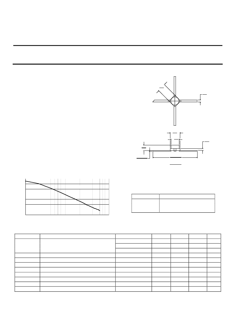
TYPICAL POWER GAIN vs FREQUENCY
35
for
increased
0
5
10
15
20
25
30
0.1
1
10
FREQUENCY (GHz)
G
Id=36mA
Ceramic Microstrip Package Outline
1,2,3
Available in short lead version as MP4TD0836.
RF OUT
AND BIAS
RF INPUT
GND
GND
2
3
1
4
.085
2,16
.100
2,55
.020
0,51
.057
1,45
.083
2,11
.455±.030
1,56 ±0,76
0.018 ±0.010
4,57 ±0,25
.006
±.002
0,15±0,05
.022
0,56
MA4TD0835
MA4TD0836
Notes:
(unless otherwise specified)
1. Dimensions are in / mm
2. Tolerance: in .xxx =
±
.005; mm .xx =
±
.13
3. See last page of data sheet for short lead Micro-X
Pin Configuration
Pin Number
1
2 & 4
3
Pin Description
RF Input
AC/DC Ground
RF Output and DC Bias
Electrical Specifications @ T
A
= +25
°
C, Id = 36 mA, Z0 = 50
Ω
Symbol
Parameters
Gp
Power Gain (
S
21
2
)
SWR
in
Input SWR
SWR
out
Output SWR
P
1 dB
Output Power @ 1 dB Gain Compression
NF
50
Ω
Noise Figure
IP
3
Third Order Intercept Point
t
D
Group Delay
V
d
Device Voltage
dV/dT
Device Voltage Temperature Coefficient
Test Conditions
f = 0.1 GHz
f = 1.0 GHz
f = 4.0 GHz
f = 0.3 to 3.0 GHz
f = 0.4 to 3.0 GHz
f = 1.0 GHz
f = 1.0 GHz
f = 1.0 GHz
f = 1.0 GHz
Units
dB
dB
dB
-
-
dBm
dB
dBm
ps
V
mV/
°
C
Min.
-
17.5
-
-
-
-
-
-
-
7.0
-
Typ.
32.5
18.5
7.0
2.0
1.5
13.5
3.2
27.0
125
7.8
-17.0
Max.
-
19.0
-
-
-
-
-
-
-
8.4
-
-
-
相關(guān)PDF資料 |
PDF描述 |
|---|---|
| MP4TD1120 | Silicon Bipolar MMIC Cascadable Amplifier |
| MP4TD0870 | Silicon Bipolar MMIC Cascadable Amplifier |
| MP4TD0870T | Silicon Bipolar MMIC Cascadable Amplifier |
| MP4TD0900 | Silicon Bipolar MMIC Cascadable Amplifier |
| MP4TD0900G | Silicon Bipolar MMIC Cascadable Amplifier |
相關(guān)代理商/技術(shù)參數(shù) |
參數(shù)描述 |
|---|---|
| MP4TD0870 | 制造商:MPLUSE 制造商全稱:MPLUSE 功能描述:Silicon Bipolar MMIC Cascadable Amplifier |
| MP4TD0870T | 制造商:MPLUSE 制造商全稱:MPLUSE 功能描述:Silicon Bipolar MMIC Cascadable Amplifier |
| MP4TD0900 | 制造商:MPLUSE 制造商全稱:MPLUSE 功能描述:Silicon Bipolar MMIC Cascadable Amplifier |
| MP4TD0900G | 制造商:MPLUSE 制造商全稱:MPLUSE 功能描述:Silicon Bipolar MMIC Cascadable Amplifier |
| MP4TD0900W | 制造商:MPLUSE 制造商全稱:MPLUSE 功能描述:Silicon Bipolar MMIC Cascadable Amplifier |
發(fā)布緊急采購,3分鐘左右您將得到回復(fù)。