- 您現(xiàn)在的位置:買賣IC網(wǎng) > PDF目錄384742 > MP1S (Mitel Networks Corporation) Quadrature Downconverter PDF資料下載
參數(shù)資料
| 型號: | MP1S |
| 廠商: | Mitel Networks Corporation |
| 英文描述: | Quadrature Downconverter |
| 中文描述: | 正交下變頻器 |
| 文件頁數(shù): | 15/20頁 |
| 文件大小: | 566K |
| 代理商: | MP1S |
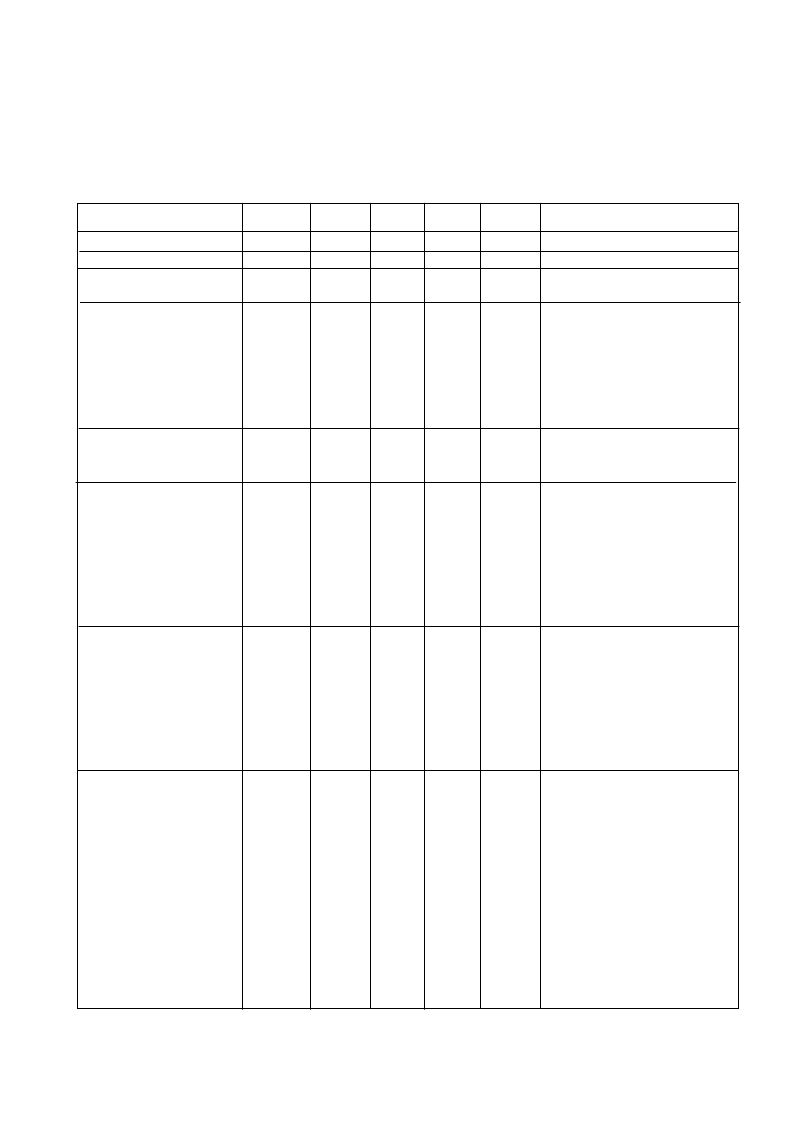
15
SL1711
ELECTRICAL CHARACTERISTICS
Test conditions (unless otherwise stated)
Tamb= 0oC to 85oC
,
*
Vee= 0V, Vcc = 4.75 to 5.25 V, Fif = 479.5 MHz, IF bandwidth
±
22 MHz, output amplitude -11dBV
These characteristics are guaranteed by either production test or design. They apply within the specified ambient temperature
and supply voltage unless otherwise stated.
Characteristic
Supply voltage
Supply current
IF input operating
frequency (1)
IF input impedance
Pin
6,9,16
6,9,16
4, 5
Min
4.75
Typ
Max
5.25
125
550
Units
V
mA
MHz
Conditions
109
350
4, 5
75
Over specified frequency
operating range, see Fig. 6.
Over specified frequency
operating range, see Fig. 6.
Maximum gain setting
Input return loss
4, 5
12
dB
Input noise figure, DSB
Variation in NF with gain
setting
VCO operation range
4, 5
17
19
1
dB
dB/dB
350
550
MHz
Centre frequency and tuning
range determined by
application.
Varactor tuned, determined
by application.
Free running
Uncompensated
VCO phase noise, SSB
@ 10kHz offset
VCO Vcc sensitivity
VCO temperature
stability
Prescaler output swing
Prescaler output duty
cycle
Conversion gain for
AGC setting of;
96
-85
dBc/Hz
2E3
100
ppm/V
ppm/
°
C
10, 11
10, 11
1.2
40
1.6
50
Vp-p
%
60
See Fig. 4
1.5V
44
dB
Terminated voltage
conversion gain from 50
source to 1k
load
2.5V
3.5V
38
dB
dB
μ
A
dB
dB
deg
dB
dB
dB
28
100
±
1
±
1
±
3
±
1
±
1
-20
AGC input current
I Q gain match
I Q gain match
I Q phase match
I & Q channel in band ripple
I & Q channel in band ripple
I Q crosstalk
1
All AGC settings
See Note 3.
See Note 4.
See Note 4.
see Note 3.
See Note 4.
See Note 4 and Note 2 for
derivation of cross modulation
±
0.3
±
0.5
±
1.5
±
0.3
±
0.5
-29
相關(guān)PDF資料 |
PDF描述 |
|---|---|
| MP1T | Quadrature Downconverter |
| MP30 | Power Rheostats 150 Watt |
| MP30A25 | Power Rheostats 150 Watt |
| MPAD | Quadrature Downconverter |
| MPAS | Quadrature Downconverter |
相關(guān)代理商/技術(shù)參數(shù) |
參數(shù)描述 |
|---|---|
| MP1SML | 制造商:CIT 制造商全稱:CIT Relay & Switch 功能描述:CIT SWITCH |
| MP1SMLC01 | 制造商:CIT 制造商全稱:CIT Relay & Switch 功能描述:CIT SWITCH |
| MP1SMLC02 | 制造商:CIT 制造商全稱:CIT Relay & Switch 功能描述:CIT SWITCH |
| MP1SMLC03 | 制造商:CIT 制造商全稱:CIT Relay & Switch 功能描述:CIT SWITCH |
| MP1SMLC04 | 制造商:CIT 制造商全稱:CIT Relay & Switch 功能描述:CIT SWITCH |
發(fā)布緊急采購,3分鐘左右您將得到回復(fù)。