- 您現(xiàn)在的位置:買(mǎi)賣(mài)IC網(wǎng) > PDF目錄371127 > MMUN2111LT1 (ON SEMICONDUCTOR) PNP SILICON BIAS RESISTOR TRANSISTOR PDF資料下載
參數(shù)資料
| 型號(hào): | MMUN2111LT1 |
| 廠商: | ON SEMICONDUCTOR |
| 元件分類(lèi): | 小信號(hào)晶體管 |
| 英文描述: | PNP SILICON BIAS RESISTOR TRANSISTOR |
| 中文描述: | 100 mA, 50 V, PNP, Si, SMALL SIGNAL TRANSISTOR, TO-236AB |
| 封裝: | CASE 318-08, TO-236, 3 PIN |
| 文件頁(yè)數(shù): | 1/10頁(yè) |
| 文件大小: | 267K |
| 代理商: | MMUN2111LT1 |
1
Motorola Small–Signal Transistors, FETs and Diodes Device Data
PNP Silicon Surface Mount Transistor with
Monolithic Bias Resistor Network
This new series of digital transistors is designed to replace a single device and its
external resistor bias network. The BRT (Bias Resistor Transistor) contains a single
transistor with a monolithic bias network consisting of two resistors; a series base
resistor and a base-emitter resistor. The BRT eliminates these individual components
by integrating them into a single device. The use of a BRT can reduce both system
cost and board space. The device is housed in the SOT-23 package which is
designed for low power surface mount applications.
Simplifies Circuit Design
Reduces Board Space
Reduces Component Count
The SOT-23 package can be soldered using wave or
reflow. The modified gull-winged leads absorb thermal
stress during soldering eliminating the possibility of
damage to the die.
Available in 8 mm embossed tape and reel. Use the
Device Number to order the 7 inch/3000 unit reel.
Replace “T1” with “T3” in the Device Number to order
the 13 inch/10,000 unit reel.
MAXIMUM RATINGS
(TA = 25
°
C unless otherwise noted)
Rating
Symbol
Value
Unit
Collector-Base Voltage
VCBO
VCEO
IC
PD
50
Vdc
Collector-Emitter Voltage
50
Vdc
Collector Current
Total Power Dissipation @ TA = 25
°
C(1)
Derate above 25
°
C
100
mAdc
*
200
1.6
mW
mW/
°
C
THERMAL CHARACTERISTICS
Rating
Symbol
Value
Unit
Thermal Resistance — Junction-to-Ambient (surface mounted)
R
θ
JA
TJ, Tstg
625
°
C/W
Operating and Storage Temperature Range
–65 to +150
°
C
Maximum Temperature for Soldering Purposes,
Time in Solder Bath
TL
260
10
°
C
Sec
DEVICE MARKING AND RESISTOR VALUES
Device
Marking
R1 (K)
R2 (K)
MMUN2111LT1
MMUN2112LT1
MMUN2113LT1
MMUN2114LT1
MMUN2115LT1(2)
A6A
A6B
A6C
A6D
A6E
10
22
47
10
10
10
22
47
47
∞
1. Device mounted on a FR-4 glass epoxy printed circuit board using the minimum recommended footprint.
2. New devices. Updated curves to follow in subsequent data sheets.
Thermal Clad is a trademark of the Bergquist Company
Preferred
devices are Motorola recommended choices for future use and best overall value.
(Replaces MMUN2111T1/D)
Order this document
by MMUN2111LT1/D
SEMICONDUCTOR TECHNICAL DATA
PNP SILICON
BIAS RESISTOR
TRANSISTOR
Motorola Preferred Devices
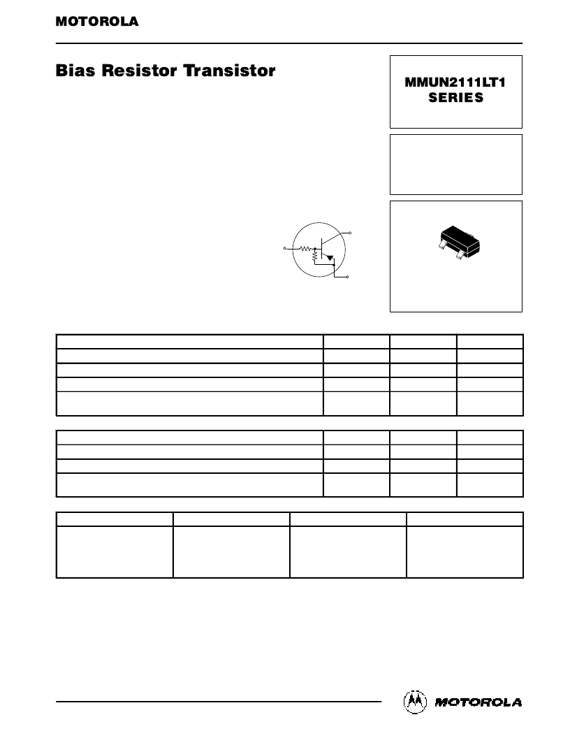
CASE 318-08, STYLE 6
SOT-23 (TO-236AB)
1
2
3
PIN 3
COLLECTOR
(OUTPUT)
PIN 2
EMITTER
(GROUND)
PIN 1
BASE
(INPUT)
R1
R2
相關(guān)PDF資料 |
PDF描述 |
|---|---|
| MMUN2113LT1 | PNP SILICON BIAS RESISTOR TRANSISTOR |
| MMUN2114LT1 | PNP SILICON BIAS RESISTOR TRANSISTOR |
| MMUN2115LT1 | PNP SILICON BIAS RESISTOR TRANSISTOR |
| MMUN2130LT1 | PNP SILICON BIAS RESISTOR TRANSISTOR |
| MMUN2116LT1 | PNP SILICON BIAS RESISTOR TRANSISTOR |
相關(guān)代理商/技術(shù)參數(shù) |
參數(shù)描述 |
|---|---|
| MMUN2111LT1_05 | 制造商:ONSEMI 制造商全稱(chēng):ON Semiconductor 功能描述:Bias Resistor Transistors |
| MMUN2111LT1G | 功能描述:開(kāi)關(guān)晶體管 - 偏壓電阻器 100mA 50V BRT PNP RoHS:否 制造商:ON Semiconductor 配置: 晶體管極性:NPN/PNP 典型輸入電阻器: 典型電阻器比率: 安裝風(fēng)格:SMD/SMT 封裝 / 箱體: 直流集電極/Base Gain hfe Min:200 mA 最大工作頻率: 集電極—發(fā)射極最大電壓 VCEO:50 V 集電極連續(xù)電流:150 mA 峰值直流集電極電流: 功率耗散:200 mW 最大工作溫度: 封裝:Reel |
| MMUN2111LT3 | 功能描述:開(kāi)關(guān)晶體管 - 偏壓電阻器 100mA 50V BRT PNP RoHS:否 制造商:ON Semiconductor 配置: 晶體管極性:NPN/PNP 典型輸入電阻器: 典型電阻器比率: 安裝風(fēng)格:SMD/SMT 封裝 / 箱體: 直流集電極/Base Gain hfe Min:200 mA 最大工作頻率: 集電極—發(fā)射極最大電壓 VCEO:50 V 集電極連續(xù)電流:150 mA 峰值直流集電極電流: 功率耗散:200 mW 最大工作溫度: 封裝:Reel |
| MMUN2111LT3G | 功能描述:開(kāi)關(guān)晶體管 - 偏壓電阻器 100mA 50V BRT PNP RoHS:否 制造商:ON Semiconductor 配置: 晶體管極性:NPN/PNP 典型輸入電阻器: 典型電阻器比率: 安裝風(fēng)格:SMD/SMT 封裝 / 箱體: 直流集電極/Base Gain hfe Min:200 mA 最大工作頻率: 集電極—發(fā)射極最大電壓 VCEO:50 V 集電極連續(xù)電流:150 mA 峰值直流集電極電流: 功率耗散:200 mW 最大工作溫度: 封裝:Reel |
| MMUN2111RLT1 | 制造商:LRC 制造商全稱(chēng):Leshan Radio Company 功能描述:Bias Resistor Transistor |
發(fā)布緊急采購(gòu),3分鐘左右您將得到回復(fù)。