- 您現(xiàn)在的位置:買賣IC網(wǎng) > PDF目錄358174 > MG-3510DC-FREQ-OUT23 CRYSTAL OSCILLATOR, CLOCK, 6 MHz - 13 MHz, CMOS/TTL OUTPUT PDF資料下載
參數(shù)資料
| 型號(hào): | MG-3510DC-FREQ-OUT23 |
| 元件分類: | XO, clock |
| 英文描述: | CRYSTAL OSCILLATOR, CLOCK, 6 MHz - 13 MHz, CMOS/TTL OUTPUT |
| 文件頁(yè)數(shù): | 1/2頁(yè) |
| 文件大?。?/td> | 74K |
| 代理商: | MG-3510DC-FREQ-OUT23 |
48
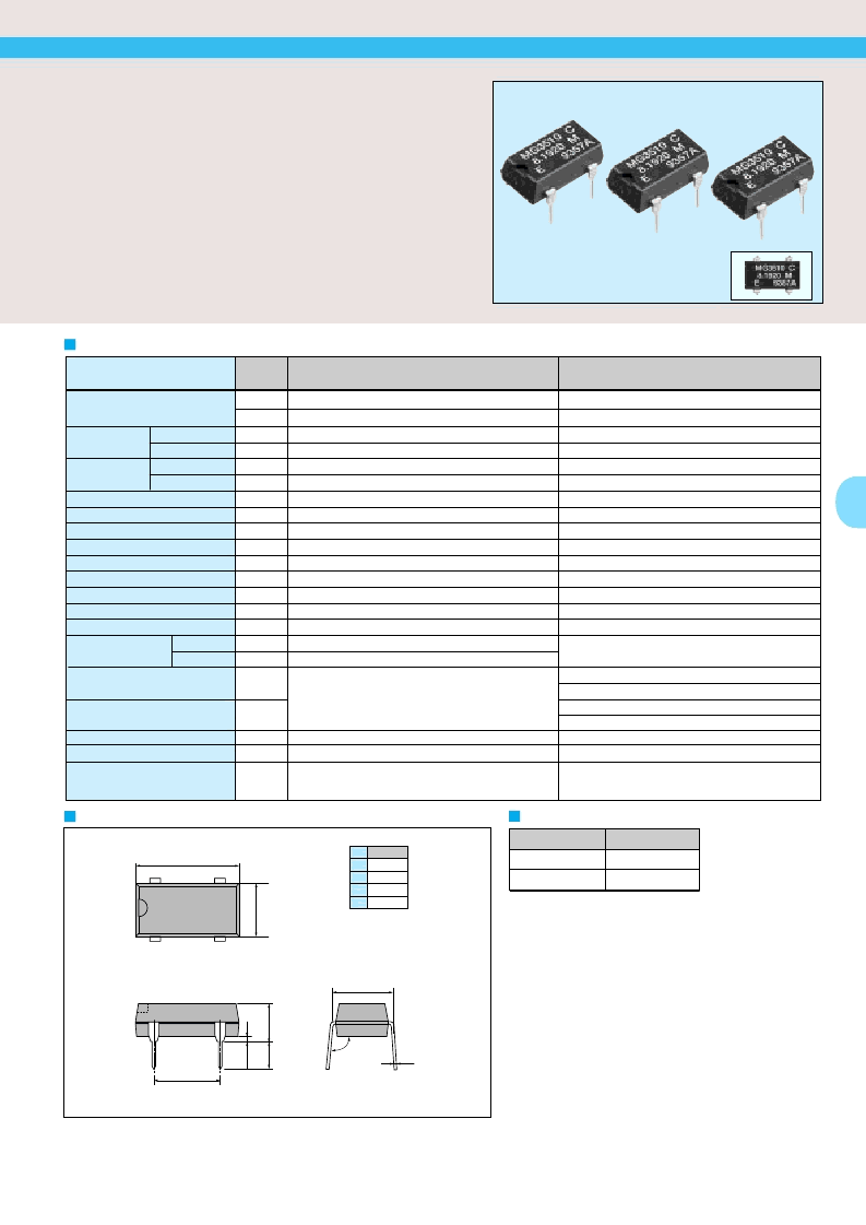
Crystal oscillator
Standard frequency
1 GND
4 OUT
1
5 OUT
2
8 V
DD
NO.
External dimensions
Specifications (characteristics)
(Unit: mm)
# 8
# 5
# 1
# 4
8.1920MHz
8.0000MHz
4.0960MHz
4.0000MHz
OUT
1
(f
1
)
OUT
2
(f
2
)
5
2
0
0.25
90 to
105
7.62
7.62
13.7max.
6
8.1920 M
E
9357A
MG3510
C
Pin terminal
MULTI-OUTPUT CRYSTAL OSCILLATOR
MG-3510DC
Simultaneous output.(1/1,1/2 output frequency ratio)
Use of C-MOS IC assures low current consumption.
Excellent shock resistance and environmental capability.
Pin compatible with half size.
Item
Output frequency range
Power source
voltage
Temperature
range
Soldering condition
Frequency stability
Current consumption
Duty
“H” output voltage 1
“L” output voltage 1
“H” output voltage 2
“L” output voltage2
Output load
condition (fan out)
Output rise time
Output fall time
Oscillation start up time
Aging
Shock resistance
Symbol
f
1
f
2
V
DD
-GND
V
DD
T
STG
T
OPR
T
SOL
f/f
0
lop
t
W
/
t
V
OH1
V
OL1
V
OH2
V
OL2
t
sk
N
C
L
t
TLH
t
THL
t
OSC
fa
S.R.
Specifications
6.0000 MHz to 13.0000 MHz
3.0000 MHz to 6.5000 MHz
-0.5V to +7.0V
5.0V ±0.5V
-55C to +100C
-10C to +70C
Under 260C within 10 sec.Package should be less than 150C
±100ppm
7mA max.
40% to 60%
0.9V
DD
min.
0.1V
DD
max.
2.4V min.
0.4V max.
20ns max.
2TTL max.
15pF. max.
10ns. max.
10ns. max.
±5ppm/year max.
±20ppm max.
Remarks
OUT
1
( f
1
)
OUT
2
(f
2
=
f
1
x 1/2
)
No load,f
1
=8.192MHz or 8.0000MHz
TTL load: 1.4V,C-MOS load :1/2V
DD
level
I
OH
= -1.0mA
I
OL
=3.2mA
I
OH
= -1.0mA
I
OL
=3.2mA
Between OUT
1
and OUT
2
Max. frequency and max. operating voltage range
C-MOS load: 10
%
→
90
%
V
DD
TTL load: 0.4V
→
2.4V
C-MOS load: 90
%
→
10
%
V
DD
TTL load: 2.4V
→
0.4V
V
DD
=4.5V voltage, t=0
Ta=25C, V
DD
=5V, first year
Three drops on a hard board from 75 cm or
excitation test with 3000G x 0.3ms x 1/2sine
wave in 3 directions
Max. supply voltage
Operating voltage
Storage temperature
Operating temperature
Actual size
TTL
C-MOS
相關(guān)PDF資料 |
PDF描述 |
|---|---|
| MG-7010SA | CRYSTAL OSCILLATOR, CLOCK, CMOS OUTPUT |
| MG150Q1JS40 | 150 A, 1200 V, N-CHANNEL IGBT |
| MG200 | EnFlex MG-200 Control Server Gateway |
| MG200_1 | 2400 MHz Mobile Antenna |
| MG47D | T-1 3/4 SINGLE COLOR LED, GREEN, 4.7 mm |
相關(guān)代理商/技術(shù)參數(shù) |
參數(shù)描述 |
|---|---|
| MG356A | 制造商:MICRO-ELECTRONICS 制造商全稱:Micro Electronics 功能描述:0.56 THREE DIGIT NUMERIC DISPLAYS |
| MG356C | 制造商:MICRO-ELECTRONICS 制造商全稱:Micro Electronics 功能描述:0.56 THREE DIGIT NUMERIC DISPLAYS |
| MG360V1US41 | 制造商:TOSHIBA 制造商全稱:Toshiba Semiconductor 功能描述:N CHANNEL IGBT (HIGH POWER SWITCHING, MOTOR CONTROL APPLICATIONS) |
| MG-37 | 制造商:MG Electronics 功能描述:BNC Video Balun |
| MG370104 | 制造商:CITIZEN 功能描述:CRYSTAL |
發(fā)布緊急采購(gòu),3分鐘左右您將得到回復(fù)。