- 您現(xiàn)在的位置:買賣IC網(wǎng) > PDF目錄45312 > MCF5473VR200 (FREESCALE SEMICONDUCTOR INC) 32-BIT, 200 MHz, RISC PROCESSOR, PBGA388 PDF資料下載
參數(shù)資料
| 型號(hào): | MCF5473VR200 |
| 廠商: | FREESCALE SEMICONDUCTOR INC |
| 元件分類: | 微控制器/微處理器 |
| 英文描述: | 32-BIT, 200 MHz, RISC PROCESSOR, PBGA388 |
| 封裝: | 27 X 27 MM, MS-034AAL-1, PBGA-388 |
| 文件頁(yè)數(shù): | 8/34頁(yè) |
| 文件大?。?/td> | 600K |
| 代理商: | MCF5473VR200 |
第1頁(yè)第2頁(yè)第3頁(yè)第4頁(yè)第5頁(yè)第6頁(yè)第7頁(yè)當(dāng)前第8頁(yè)第9頁(yè)第10頁(yè)第11頁(yè)第12頁(yè)第13頁(yè)第14頁(yè)第15頁(yè)第16頁(yè)第17頁(yè)第18頁(yè)第19頁(yè)第20頁(yè)第21頁(yè)第22頁(yè)第23頁(yè)第24頁(yè)第25頁(yè)第26頁(yè)第27頁(yè)第28頁(yè)第29頁(yè)第30頁(yè)第31頁(yè)第32頁(yè)第33頁(yè)第34頁(yè)
MCF547x ColdFire Microprocessor, Rev. 4
SDRAM Bus
Freescale Semiconductor
16
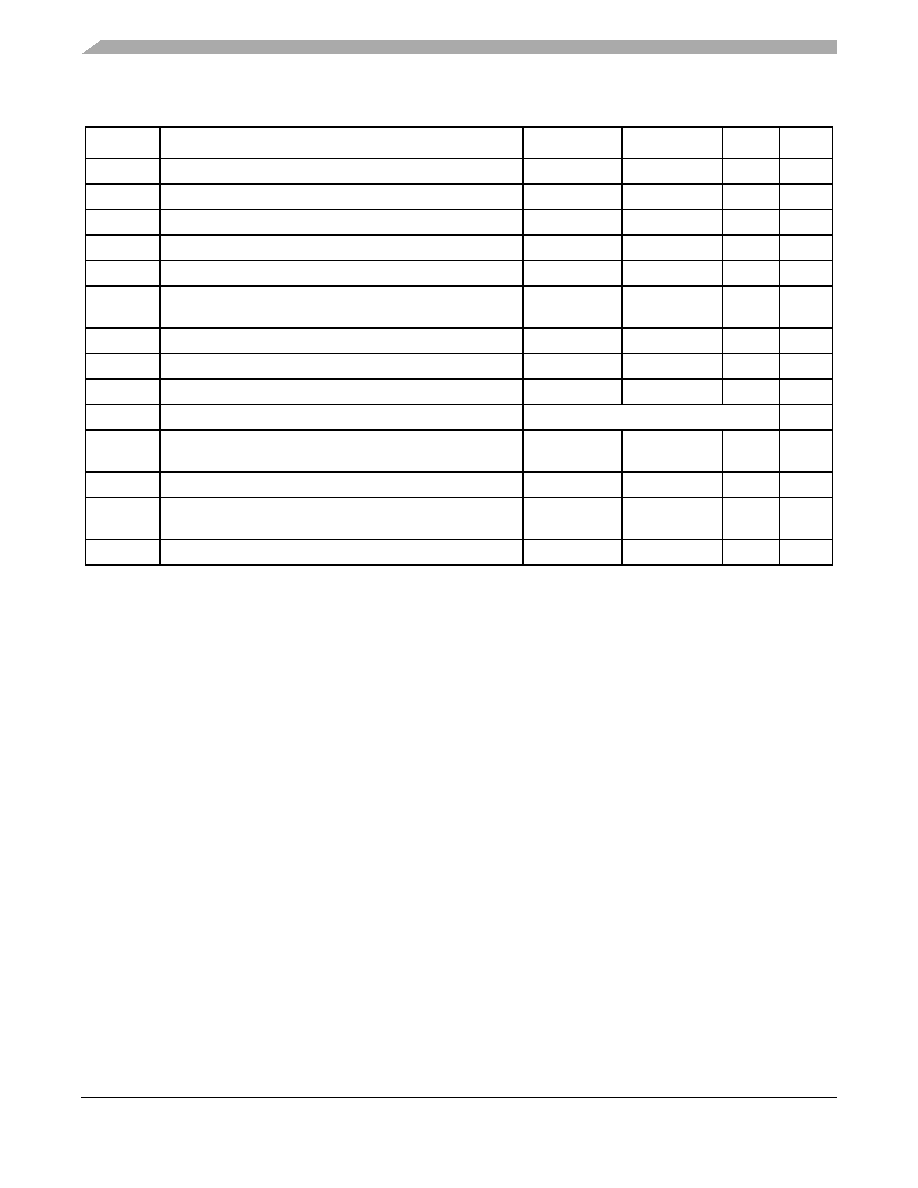
Table 11. SDR Timing Specifications
Symbol
Characteristic
Min
Max
Unit
Notes
Frequency of Operation
0
133
Mhz
1
1 The frequency of operation is 2x or 4x the CLKIN frequency of operation. The MCF547X supports a single external reference
clock (CLKIN). This signal defines the frequency of operation for FlexBus and PCI, but SDRAM clock operates at the same
frequency as the internal bus clock. Please see the PLL chapter of the MCF547X Reference Manual for more information on
setting the SDRAM clock rate.
SD1
Clock Period (tCK)7.52
12
ns
2
2 SDCLK is one SDRAM clock in (ns).
SD2
Clock Skew (tSK)TBD
SD3
Pulse Width High (tCKH)
0.45
0.55
SDCLK
3
3 Pulse width high plus pulse width low cannot exceed min and max clock period.
SD4
Pulse Width Low (tCKL)
0.45
0.55
SDCLK
4
4 Pulse width high plus pulse width low cannot exceed min and max clock period.
SD5
Address, CKE, CAS, RAS, WE, BA, CS - Output Valid (tCMV)0.5 × SDCLK +
1.0ns
ns
SD6
Address, CKE, CAS, RAS, WE, BA, CS - Output Hold (tCMH)2.0
ns
SD7
SDRDQS Output Valid (tDQSOV)Self timed
ns
5
5 SDR_DQS is designed to pulse 0.25 clock before the rising edge of the memory clock. This is a guideline only. Subtle
variation from this guideline is expected. SDR_DQS only pulses during a read cycle and one pulse occurs for each data beat.
SD8
SDDQS[3:0] input setup relative to SDCLK (tDQSIS)0.25 × SDCLK 0.40 × SDCLK
ns
6
6 SDR_DQS is designed to pulse 0.25 clock before the rising edge of the memory clock. This spec is a guideline only. Subtle
variation from this guideline is expected. SDR_DQS only pulses during a read cycle and one pulse occurs for each data beat.
SD9
SDDQS[3:0] input hold relative to SDCLK (tDQSIH)
Does not apply. 0.5 SDCLK fixed width.
7
7 The SDR_DQS pulse is designed to be 0.5 clock in width. The timing of the rising edge is most important. The falling edge
does not affect the memory controller.
SD10
Data Input Setup relative to SDCLK (reference only) (tDIS)0.25 × SDCLK
ns
8
8 Because a read cycle in SDR mode uses the DQS circuit within the MCF547X, it is most critical that the data valid window
be centered 1/4 clk after the rising edge of DQS. Ensuring that this happens results in successful SDR reads. The input setup
spec is provided as guidance.
SD11
Data Input Hold relative to SDCLK (reference only) (tDIH)1.0
ns
SD12
Data and Data Mask Output Valid (tDV)0.75 × SDCLK
+0.500ns
ns
SD13
Data and Data Mask Output Hold (tDH)1.5
ns
相關(guān)PDF資料 |
PDF描述 |
|---|---|
| MCF5481CZP166 | 32-BIT, 166.66 MHz, RISC PROCESSOR, PBGA388 |
| MCF5484CZP200 | 32-BIT, 200 MHz, RISC PROCESSOR, PBGA388 |
| MCF5485CVR200 | 32-BIT, 200 MHz, RISC PROCESSOR, PBGA388 |
| MCF5483CVR166 | 32-BIT, 166.66 MHz, RISC PROCESSOR, PBGA388 |
| MCF5481CZP166 | 32-BIT, 166.66 MHz, RISC PROCESSOR, PBGA388 |
相關(guān)代理商/技術(shù)參數(shù) |
參數(shù)描述 |
|---|---|
| MCF5473ZP200 | 功能描述:微處理器 - MPU MCF547X V4ECORE MMU FPU RoHS:否 制造商:Atmel 處理器系列:SAMA5D31 核心:ARM Cortex A5 數(shù)據(jù)總線寬度:32 bit 最大時(shí)鐘頻率:536 MHz 程序存儲(chǔ)器大小:32 KB 數(shù)據(jù) RAM 大小:128 KB 接口類型:CAN, Ethernet, LIN, SPI,TWI, UART, USB 工作電源電壓:1.8 V to 3.3 V 最大工作溫度:+ 85 C 安裝風(fēng)格:SMD/SMT 封裝 / 箱體:FBGA-324 |
| MCF5474 | 制造商:FREESCALE 制造商全稱:Freescale Semiconductor, Inc 功能描述:MCF547x Integrated Microprocessor Electrical Characteristics |
| MCF5474EC | 制造商:FREESCALE 制造商全稱:Freescale Semiconductor, Inc 功能描述:MCF547x ColdFire Microprocessor |
| MCF5474VR200 | 功能描述:微處理器 - MPU MCF547X V4ECORE MMU FPU RoHS:否 制造商:Atmel 處理器系列:SAMA5D31 核心:ARM Cortex A5 數(shù)據(jù)總線寬度:32 bit 最大時(shí)鐘頻率:536 MHz 程序存儲(chǔ)器大小:32 KB 數(shù)據(jù) RAM 大小:128 KB 接口類型:CAN, Ethernet, LIN, SPI,TWI, UART, USB 工作電源電壓:1.8 V to 3.3 V 最大工作溫度:+ 85 C 安裝風(fēng)格:SMD/SMT 封裝 / 箱體:FBGA-324 |
| MCF5474VR266 | 功能描述:微處理器 - MPU MCF547X V4ECORE MMU FPU RoHS:否 制造商:Atmel 處理器系列:SAMA5D31 核心:ARM Cortex A5 數(shù)據(jù)總線寬度:32 bit 最大時(shí)鐘頻率:536 MHz 程序存儲(chǔ)器大小:32 KB 數(shù)據(jù) RAM 大小:128 KB 接口類型:CAN, Ethernet, LIN, SPI,TWI, UART, USB 工作電源電壓:1.8 V to 3.3 V 最大工作溫度:+ 85 C 安裝風(fēng)格:SMD/SMT 封裝 / 箱體:FBGA-324 |
發(fā)布緊急采購(gòu),3分鐘左右您將得到回復(fù)。