- 您現(xiàn)在的位置:買賣IC網(wǎng) > PDF目錄45277 > MC8610PX800GZ (FREESCALE SEMICONDUCTOR INC) MICROPROCESSOR, PBGA783 PDF資料下載
參數(shù)資料
| 型號: | MC8610PX800GZ |
| 廠商: | FREESCALE SEMICONDUCTOR INC |
| 元件分類: | 微控制器/微處理器 |
| 英文描述: | MICROPROCESSOR, PBGA783 |
| 封裝: | 29 X 29 MM, PLASTIC, FCBGA-783 |
| 文件頁數(shù): | 24/96頁 |
| 文件大小: | 1237K |
| 代理商: | MC8610PX800GZ |
第1頁第2頁第3頁第4頁第5頁第6頁第7頁第8頁第9頁第10頁第11頁第12頁第13頁第14頁第15頁第16頁第17頁第18頁第19頁第20頁第21頁第22頁第23頁當前第24頁第25頁第26頁第27頁第28頁第29頁第30頁第31頁第32頁第33頁第34頁第35頁第36頁第37頁第38頁第39頁第40頁第41頁第42頁第43頁第44頁第45頁第46頁第47頁第48頁第49頁第50頁第51頁第52頁第53頁第54頁第55頁第56頁第57頁第58頁第59頁第60頁第61頁第62頁第63頁第64頁第65頁第66頁第67頁第68頁第69頁第70頁第71頁第72頁第73頁第74頁第75頁第76頁第77頁第78頁第79頁第80頁第81頁第82頁第83頁第84頁第85頁第86頁第87頁第88頁第89頁第90頁第91頁第92頁第93頁第94頁第95頁第96頁
MPC8610 Integrated Host Processor Hardware Specifications, Rev. 2
Electrical Characteristics
Freescale Semiconductor
30
NOTE
For the ADDR/CMD setup and hold specifications in Table 22, it is assumed that the clock
control register is set to adjust the memory clocks by 1/2 applied cycle.
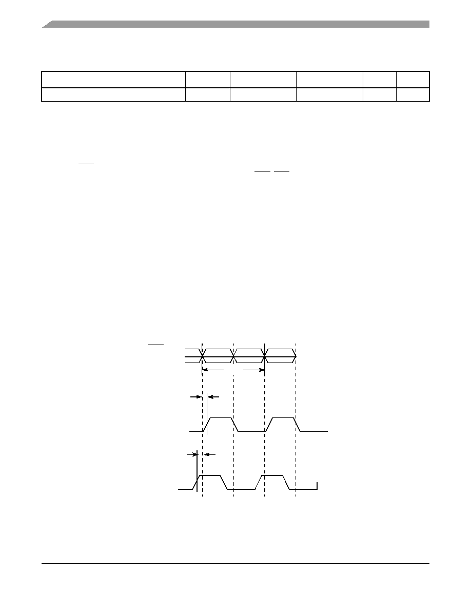
Figure 5. Timing Diagram for tDDKHMH
MDQS epilogue end
tDDKHME
–0.6
0.6
ns
6
Notes:
1. The symbols used for timing specifications follow the pattern of t(first two letters of functional block)(signal)(state)(reference)(state) for
inputs and t(first two letters of functional block)(reference)(state)(signal)(state) for outputs. Output hold time can be read as DDR timing
(DD) from the rising or falling edge of the reference clock (KH or KL) until the output went invalid (AX or DX). For example,
tDDKHAS symbolizes DDR timing (DD) for the time tMCK memory clock reference (K) goes from the high (H) state until outputs
(A) are setup (S) or output valid time. Also, tDDKLDX symbolizes DDR timing (DD) for the time tMCK memory clock reference
(K) goes low (L) until data outputs (D) are invalid (X) or data output hold time.
2. All MCK/MCK referenced measurements are made from the crossing of the two signals ±0.1 V.
3. ADDR/CMD includes all DDR SDRAM output signals except MCK/MCK, MCS, and MDQ/MECC/MDM/MDQS.
4. Note that tDDKHMH follows the symbol conventions described in note 1. For example, tDDKHMH describes the DDR timing (DD)
from the rising edge of the MCK[n] clock (KH) until the MDQS signal is valid (MH). tDDKHMH can be modified through control
of the DQSS override bits in the TIMING_CFG_2 register. This will typically be set to the same delay as the clock adjust in
the CLK_CNTL register. The timing parameters listed in the table assume that these 2 parameters have been set to the same
adjustment value. See the
MPC8610 Integrated Host Processor Reference Manual, for a description and understanding of
the timing modifications enabled by use of these bits.
5. Determined by maximum possible skew between a data strobe (MDQS) and any corresponding bit of data (MDQ), ECC
(MECC), or data mask (MDM). The data strobe should be centered inside of the data eye at the pins of the microprocessor.
6. All outputs are referenced to the rising edge of MCK[
n] at the pins of the microprocessor. Note that tDDKHMP follows the
symbol conventions described in note 1.
7. Maximum DDR1 frequency is 400 MHz.
8. Per the JEDEC spec the DDR2 duty cycle at 400 and 533 MHz is the low and high cycle time values.
Table 22. DDR SDRAM Output AC Timing Specifications (continued)
At recommended operating conditions.
Parameter
Symbol1
Min
Max
Unit
Notes
MDQS
MCK[
n]
MCK[
n]
tMCK
tDDKHMHmax) = 0.6 ns
tDDKHMH(min) = –0.6 ns
MDQS
相關PDF資料 |
PDF描述 |
|---|---|
| MC8610VT800GZ | MICROPROCESSOR, PBGA783 |
| MC8640DVU1000HE | 32-BIT, 1000 MHz, MICROPROCESSOR, CBGA1023 |
| MC8640DTHX1250HC | 32-BIT, 1250 MHz, MICROPROCESSOR, CBGA1023 |
| MC8640TVU1000HC | 32-BIT, 1000 MHz, MICROPROCESSOR, CBGA1023 |
| MC8640VU1250HC | 32-BIT, 1250 MHz, MICROPROCESSOR, CBGA1023 |
相關代理商/技術參數(shù) |
參數(shù)描述 |
|---|---|
| MC8610PX800J | 制造商:FREESCALE 制造商全稱:Freescale Semiconductor, Inc 功能描述:Integrated Host Processor Hardware Specifications |
| MC8610TPX1066JB | 功能描述:微處理器 - MPU REV 1.1 8610 1.0V -40C RoHS:否 制造商:Atmel 處理器系列:SAMA5D31 核心:ARM Cortex A5 數(shù)據(jù)總線寬度:32 bit 最大時鐘頻率:536 MHz 程序存儲器大小:32 KB 數(shù)據(jù) RAM 大小:128 KB 接口類型:CAN, Ethernet, LIN, SPI,TWI, UART, USB 工作電源電壓:1.8 V to 3.3 V 最大工作溫度:+ 85 C 安裝風格:SMD/SMT 封裝 / 箱體:FBGA-324 |
| MC8610TPX1066JZ | 制造商:FREESCALE 制造商全稱:Freescale Semiconductor, Inc 功能描述:MPC8610 Integrated Host Processor Hardware Specifications |
| MC8610TPX1067G | 制造商:FREESCALE 制造商全稱:Freescale Semiconductor, Inc 功能描述:Integrated Host Processor Hardware Specifications |
| MC8610TPX1067J | 制造商:FREESCALE 制造商全稱:Freescale Semiconductor, Inc 功能描述:Integrated Host Processor Hardware Specifications |
發(fā)布緊急采購,3分鐘左右您將得到回復。