- 您現(xiàn)在的位置:買賣IC網(wǎng) > PDF目錄45379 > MC80C32-36 (TEMIC SEMICONDUCTORS) 8-BIT, 36 MHz, MICROCONTROLLER, CDIP40 PDF資料下載
參數(shù)資料
| 型號(hào): | MC80C32-36 |
| 廠商: | TEMIC SEMICONDUCTORS |
| 元件分類: | 微控制器/微處理器 |
| 英文描述: | 8-BIT, 36 MHz, MICROCONTROLLER, CDIP40 |
| 文件頁數(shù): | 212/286頁 |
| 文件大?。?/td> | 9413K |
| 代理商: | MC80C32-36 |
第1頁第2頁第3頁第4頁第5頁第6頁第7頁第8頁第9頁第10頁第11頁第12頁第13頁第14頁第15頁第16頁第17頁第18頁第19頁第20頁第21頁第22頁第23頁第24頁第25頁第26頁第27頁第28頁第29頁第30頁第31頁第32頁第33頁第34頁第35頁第36頁第37頁第38頁第39頁第40頁第41頁第42頁第43頁第44頁第45頁第46頁第47頁第48頁第49頁第50頁第51頁第52頁第53頁第54頁第55頁第56頁第57頁第58頁第59頁第60頁第61頁第62頁第63頁第64頁第65頁第66頁第67頁第68頁第69頁第70頁第71頁第72頁第73頁第74頁第75頁第76頁第77頁第78頁第79頁第80頁第81頁第82頁第83頁第84頁第85頁第86頁第87頁第88頁第89頁第90頁第91頁第92頁第93頁第94頁第95頁第96頁第97頁第98頁第99頁第100頁第101頁第102頁第103頁第104頁第105頁第106頁第107頁第108頁第109頁第110頁第111頁第112頁第113頁第114頁第115頁第116頁第117頁第118頁第119頁第120頁第121頁第122頁第123頁第124頁第125頁第126頁第127頁第128頁第129頁第130頁第131頁第132頁第133頁第134頁第135頁第136頁第137頁第138頁第139頁第140頁第141頁第142頁第143頁第144頁第145頁第146頁第147頁第148頁第149頁第150頁第151頁第152頁第153頁第154頁第155頁第156頁第157頁第158頁第159頁第160頁第161頁第162頁第163頁第164頁第165頁第166頁第167頁第168頁第169頁第170頁第171頁第172頁第173頁第174頁第175頁第176頁第177頁第178頁第179頁第180頁第181頁第182頁第183頁第184頁第185頁第186頁第187頁第188頁第189頁第190頁第191頁第192頁第193頁第194頁第195頁第196頁第197頁第198頁第199頁第200頁第201頁第202頁第203頁第204頁第205頁第206頁第207頁第208頁第209頁第210頁第211頁當(dāng)前第212頁第213頁第214頁第215頁第216頁第217頁第218頁第219頁第220頁第221頁第222頁第223頁第224頁第225頁第226頁第227頁第228頁第229頁第230頁第231頁第232頁第233頁第234頁第235頁第236頁第237頁第238頁第239頁第240頁第241頁第242頁第243頁第244頁第245頁第246頁第247頁第248頁第249頁第250頁第251頁第252頁第253頁第254頁第255頁第256頁第257頁第258頁第259頁第260頁第261頁第262頁第263頁第264頁第265頁第266頁第267頁第268頁第269頁第270頁第271頁第272頁第273頁第274頁第275頁第276頁第277頁第278頁第279頁第280頁第281頁第282頁第283頁第284頁第285頁第286頁
31
8183F–AVR–06/12
ATtiny24A/44A/84A
6.5
Register Description
6.5.1
OSCCAL – Oscillator Calibration Register
Bits 7:0 – CAL[7:0]: Oscillator Calibration Value
The Oscillator Calibration Register is used to trim the Calibrated Internal RC Oscillator to
remove process variations from the oscillator frequency. A pre-programmed calibration value is
automatically written to this register during chip reset, giving the Factory calibrated frequency as
specified in Table 20-2 on page 175. The application software can write this register to change
the oscillator frequency. The oscillator can be calibrated to frequencies as specified in Table 20-
2 on page 175. Calibration outside that range is not guaranteed.
Note that this oscillator is used to time EEPROM and Flash write accesses, and these write
times will be affected accordingly. If the EEPROM or Flash are written, do not calibrate to more
than 8.8 MHz. Otherwise, the EEPROM or Flash write may fail.
The CAL7 bit determines the range of operation for the oscillator. Setting this bit to 0 gives the
lowest frequency range, setting this bit to 1 gives the highest frequency range. The two fre-
quency ranges are overlapping, in other words a setting of OSCCAL = 0x7F gives a higher
frequency than OSCCAL = 0x80.
The CAL[6:0] bits are used to tune the frequency within the selected range. A setting of 0x00
gives the lowest frequency in that range, and a setting of 0x7F gives the highest frequency in the
range. See “Calibrated 8 MHz RC Oscillator Frequency vs. OSCCAL Value” on page 238 for typ-
ical frequencies.
To ensure stable operation of the MCU the calibration value should be changed in small. A vari-
ation in frequency of more than 2% from one cycle to the next can lead to unpredicatble
behavior. Changes in OSCCAL should not exceed 0x20 for each calibration. It is required to
ensure that the MCU is kept in Reset during such changes in the clock frequency.
6.5.2
CLKPR – Clock Prescale Register
Bit 7 – CLKPCE: Clock Prescaler Change Enable
The CLKPCE bit must be written to logic one to enable change of the CLKPS bits. The CLKPCE
bit is only updated when the other bits in CLKPR are simultaniosly written to zero. CLKPCE is
cleared by hardware four cycles after it is written or when the CLKPS bits are written. Rewriting
the CLKPCE bit within this time-out period does neither extend the time-out period, nor clear the
CLKPCE bit.
Bits 6:4 – Res: Reserved Bits
These bits are reserved in the ATtiny24A/44A/84A and will always read as zero.
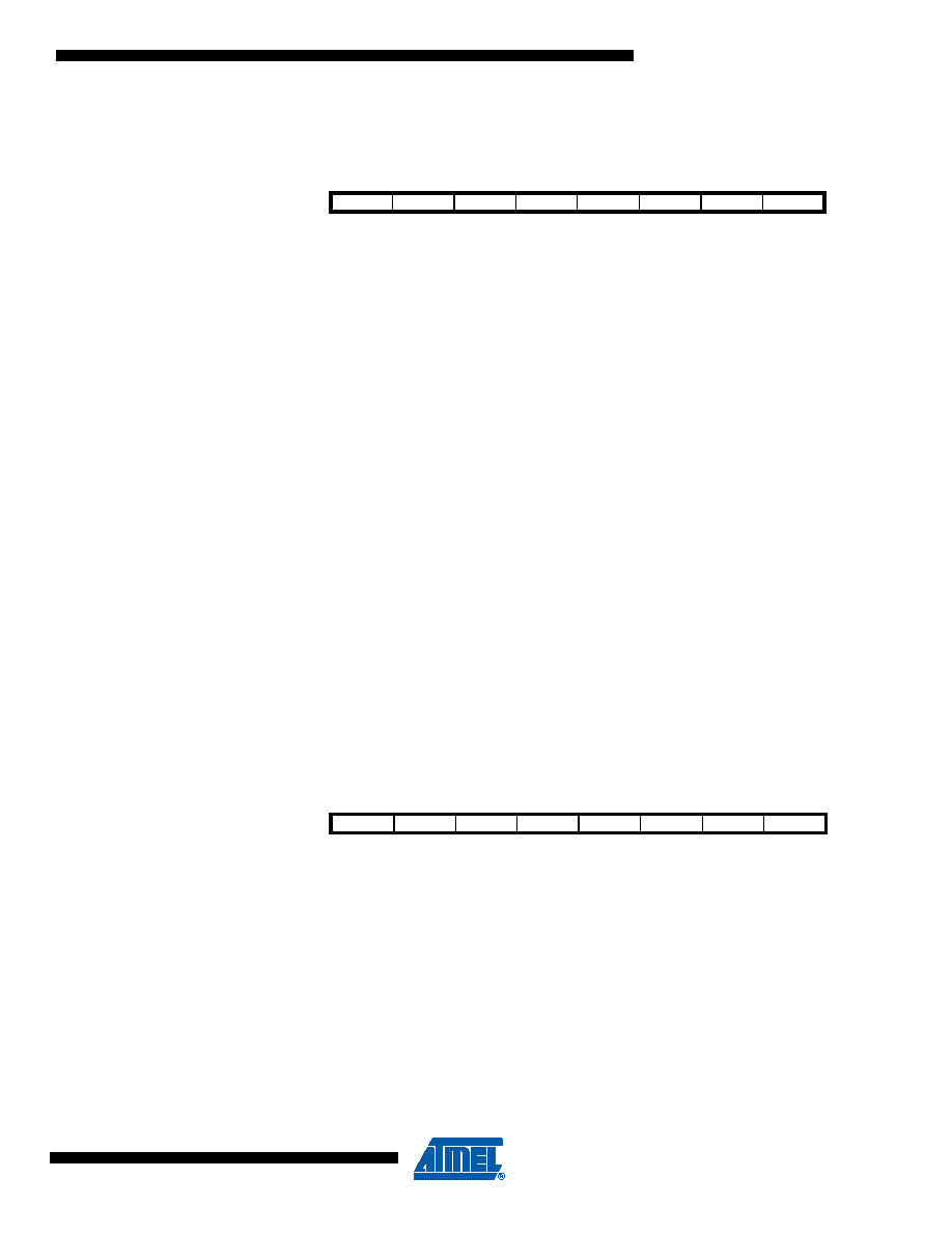
Bit
765
432
10
CAL7
CAL6
CAL5
CAL4
CAL3
CAL2
CAL1
CAL0
OSCCAL
Read/Write
R/W
Initial Value
Device Specific Calibration Value
Bit
7
6
5
4
32
10
CLKPCE
–
CLKPS3
CLKPS2
CLKPS1
CLKPS0
CLKPR
Read/Write
R/W
R
R/W
Initial Value
0
See Bit Description
相關(guān)PDF資料 |
PDF描述 |
|---|---|
| MR80C52CXXX-12SHXXX:D | 8-BIT, MROM, 12 MHz, MICROCONTROLLER, CQCC44 |
| MQ80C52TXXX-25SHXXX:R | 8-BIT, MROM, 25 MHz, MICROCONTROLLER, CQFP44 |
| MD80C32E-25SB | 8-BIT, 25 MHz, MICROCONTROLLER, CDIP40 |
| MR80C32E-30SBD | 8-BIT, 30 MHz, MICROCONTROLLER, CQCC44 |
| MR83C154DXXX-12/883R | 8-BIT, MROM, 12 MHz, MICROCONTROLLER, CQCC44 |
相關(guān)代理商/技術(shù)參數(shù) |
參數(shù)描述 |
|---|---|
| MC-80C32E-30 | 制造商:AIMTEC 制造商全稱:AIMTEC 功能描述:Rad. Tolerant 8-bit ROMless Microcontroller |
| MC-80C32E-30-E | 制造商:AIMTEC 制造商全稱:AIMTEC 功能描述:Rad. Tolerant 8-bit ROMless Microcontroller |
| MC80D21000G | 制造商:COR 功能描述:RN |
| MC80F0104 | 制造商:未知廠家 制造商全稱:未知廠家 功能描述:8-BIT SINGLE-CHIP MICROCONTROLLERS |
| MC80F0104B | 制造商:未知廠家 制造商全稱:未知廠家 功能描述:8-BIT SINGLE-CHIP MICROCONTROLLERS |
發(fā)布緊急采購,3分鐘左右您將得到回復(fù)。