- 您現(xiàn)在的位置:買賣IC網(wǎng) > PDF目錄383565 > MC74ACT574DTR2G (ON SEMICONDUCTOR) Octal D Flip−Flop with 3−State Outputs PDF資料下載
參數(shù)資料
| 型號(hào): | MC74ACT574DTR2G |
| 廠商: | ON SEMICONDUCTOR |
| 元件分類: | 通用總線功能 |
| 英文描述: | Octal D Flip−Flop with 3−State Outputs |
| 中文描述: | ACT SERIES, 8-BIT DRIVER, TRUE OUTPUT, PDSO20 |
| 封裝: | LEAD FREE, TSSOP-20 |
| 文件頁數(shù): | 2/10頁 |
| 文件大?。?/td> | 125K |
| 代理商: | MC74ACT574DTR2G |
MC74AC574, MC74ACT574
http://onsemi.com
2
FUNCTIONAL DESCRIPTION
The MC74AC574/74ACT574 consists of eight edge-
triggered flipflops with individual Dtype inputs and
3state true outputs. The buffered clock and buffered Output
Enable are common to all flipflops. The eight flipflops
will store the state of their individual D inputs that meet the
setup and hold time requirements on the LOWtoHIGH
Clock (CP) transition. With the Output Enable (OE) LOW,
the contents of the eight flipflops are available at the
outputs. When OE is HIGH, the outputs go to the high
impedance state. Operation of the OE input does not affect
the state of the flipflops.
FUNCTION TABLE
Inputs
Internal
Outputs
Function
OE
CP
D
Q
O
n
H
H
H
H
L
L
L
L
H
H
L
H
L
H
L
H
L
H
NC
NC
L
H
L
H
NC
NC
Z
Z
Z
Z
L
H
NC
NC
Hold
Hold
Load
Load
Data Available
Data Available
No Change in Data
No Change in Data
H
H
H = HIGH Voltage Level
L = LOW Voltage Level
X = Immaterial
Z = High Impedance
= LOW-to-HIGH Clock Transition
NC = No Change
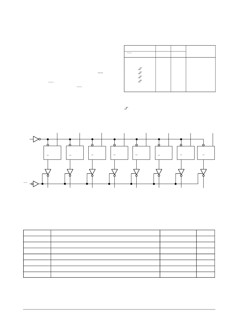
Figure 3. Logic Diagram
D
0
D
1
D
2
D
3
D
4
D
5
D
6
D
7
C
D
Q
O
0
O
1
O
2
O
3
O
4
O
5
O
6
O
7
OE
CP
C
D
Q
C
D
Q
C
D
Q
C
D
Q
C
D
Q
C
D
Q
C
D
Q
NOTE:
This diagram is provided only for the understanding of logic operations
and should not be used to estimate propagation delays.
MAXIMUM RATINGS
Symbol
Parameter
Value
Unit
V
CC
DC Supply Voltage (Referenced to GND)
0.5 to +7.0
V
V
IN
DC Input Voltage (Referenced to GND)
0.5 to V
CC
+0.5
V
V
OUT
DC Output Voltage (Referenced to GND)
0.5 to V
CC
+0.5
V
I
IN
DC Input Current, per Pin
±
20
mA
I
OUT
DC Output Sink/Source Current, per Pin
±
50
mA
I
CC
DC V
CC
or GND Current per Output Pin
±
50
mA
T
stg
Storage Temperature
65 to +150
°
C
Stresses exceeding Maximum Ratings may damage the device. Maximum Ratings are stress ratings only. Functional operation above the
Recommended Operating Conditions is not implied. Extended exposure to stresses above the Recommended Operating Conditions may affect
device reliability.
相關(guān)PDF資料 |
PDF描述 |
|---|---|
| MC74ACT574DWG | Octal D Flip−Flop with 3−State Outputs |
| MC74ACT574DWR2G | Octal D Flip−Flop with 3−State Outputs |
| MC74ACT574MELG | Octal D Flip−Flop with 3−State Outputs |
| MC74ACT574MG | Octal D Flip−Flop with 3−State Outputs |
| MC74ACT574NG | Octal D Flip−Flop with 3−State Outputs |
相關(guān)代理商/技術(shù)參數(shù) |
參數(shù)描述 |
|---|---|
| MC74ACT574DW | 功能描述:觸發(fā)器 5V CMOS Octal RoHS:否 制造商:Texas Instruments 電路數(shù)量:2 邏輯系列:SN74 邏輯類型:D-Type Flip-Flop 極性:Inverting, Non-Inverting 輸入類型:CMOS 輸出類型: 傳播延遲時(shí)間:4.4 ns 高電平輸出電流:- 16 mA 低電平輸出電流:16 mA 電源電壓-最大:5.5 V 最大工作溫度:+ 85 C 安裝風(fēng)格:SMD/SMT 封裝 / 箱體:X2SON-8 封裝:Reel |
| MC74ACT574DWG | 功能描述:觸發(fā)器 5V CMOS Octal D-Type 3-State Out RoHS:否 制造商:Texas Instruments 電路數(shù)量:2 邏輯系列:SN74 邏輯類型:D-Type Flip-Flop 極性:Inverting, Non-Inverting 輸入類型:CMOS 輸出類型: 傳播延遲時(shí)間:4.4 ns 高電平輸出電流:- 16 mA 低電平輸出電流:16 mA 電源電壓-最大:5.5 V 最大工作溫度:+ 85 C 安裝風(fēng)格:SMD/SMT 封裝 / 箱體:X2SON-8 封裝:Reel |
| MC74ACT574DWR2 | 功能描述:觸發(fā)器 5V CMOS Octal RoHS:否 制造商:Texas Instruments 電路數(shù)量:2 邏輯系列:SN74 邏輯類型:D-Type Flip-Flop 極性:Inverting, Non-Inverting 輸入類型:CMOS 輸出類型: 傳播延遲時(shí)間:4.4 ns 高電平輸出電流:- 16 mA 低電平輸出電流:16 mA 電源電壓-最大:5.5 V 最大工作溫度:+ 85 C 安裝風(fēng)格:SMD/SMT 封裝 / 箱體:X2SON-8 封裝:Reel |
| MC74ACT574DWR2G | 功能描述:觸發(fā)器 5V CMOS Octal D-Type 3-State Out RoHS:否 制造商:Texas Instruments 電路數(shù)量:2 邏輯系列:SN74 邏輯類型:D-Type Flip-Flop 極性:Inverting, Non-Inverting 輸入類型:CMOS 輸出類型: 傳播延遲時(shí)間:4.4 ns 高電平輸出電流:- 16 mA 低電平輸出電流:16 mA 電源電壓-最大:5.5 V 最大工作溫度:+ 85 C 安裝風(fēng)格:SMD/SMT 封裝 / 箱體:X2SON-8 封裝:Reel |
| MC74ACT574M | 功能描述:觸發(fā)器 5V CMOS Octal RoHS:否 制造商:Texas Instruments 電路數(shù)量:2 邏輯系列:SN74 邏輯類型:D-Type Flip-Flop 極性:Inverting, Non-Inverting 輸入類型:CMOS 輸出類型: 傳播延遲時(shí)間:4.4 ns 高電平輸出電流:- 16 mA 低電平輸出電流:16 mA 電源電壓-最大:5.5 V 最大工作溫度:+ 85 C 安裝風(fēng)格:SMD/SMT 封裝 / 箱體:X2SON-8 封裝:Reel |
發(fā)布緊急采購(gòu),3分鐘左右您將得到回復(fù)。