- 您現(xiàn)在的位置:買賣IC網(wǎng) > PDF目錄383563 > MC74AC299N (ON SEMICONDUCTOR) 8−Input Universal Shift/Storage Register with Common Parallel I/O Pins PDF資料下載
參數(shù)資料
| 型號(hào): | MC74AC299N |
| 廠商: | ON SEMICONDUCTOR |
| 元件分類: | 通用總線功能 |
| 英文描述: | 8−Input Universal Shift/Storage Register with Common Parallel I/O Pins |
| 中文描述: | AC SERIES, 8-BIT BIDIRECTIONAL PARALLEL IN PARALLEL OUT SHIFT REGISTER, TRUE OUTPUT, PDIP20 |
| 封裝: | PLASTIC, DIP-20 |
| 文件頁(yè)數(shù): | 3/11頁(yè) |
| 文件大小: | 268K |
| 代理商: | MC74AC299N |
MC74AC299, MC74ACT299
http://onsemi.com
3
FUNCTIONAL DESCRIPTION
The MC74AC299/74ACT299 contains eight edge
triggered
D
type flip
flops and the interstage logic necessary to
perform synchronous shift left, shift right, parallel load and
hold operations. The type of operation is determined by S
0
and S
1
, as shown in the Truth Table. All flip
flop outputs are
brought out through 3
state buffers to separate I/O pins that
also serve as data inputs in the parallel load mode. Q
0
and Q
7
are also brought out on other pins for expansion in serial
shifting of longer words.
A LOW signal on MR overrides the Select and CP inputs
and resets the flip
flops. All other state changes are initiated
by the rising edge of the clock. Inputs can change when the
clock is in either state provided only that the recommended
setup and hold times, relative to the rising edge of CP, are
observed.
A HIGH signal on either OE
1
or OE
2
disables the 3
-
state
buffers and puts the I/O pins in the high impedance state. In
this condition the shift, hold, load and reset operations can
still occur. The 3
state buffers are also disabled by HIGH
signals on both S
0
and S
1
in preparation for a parallel load
operation.
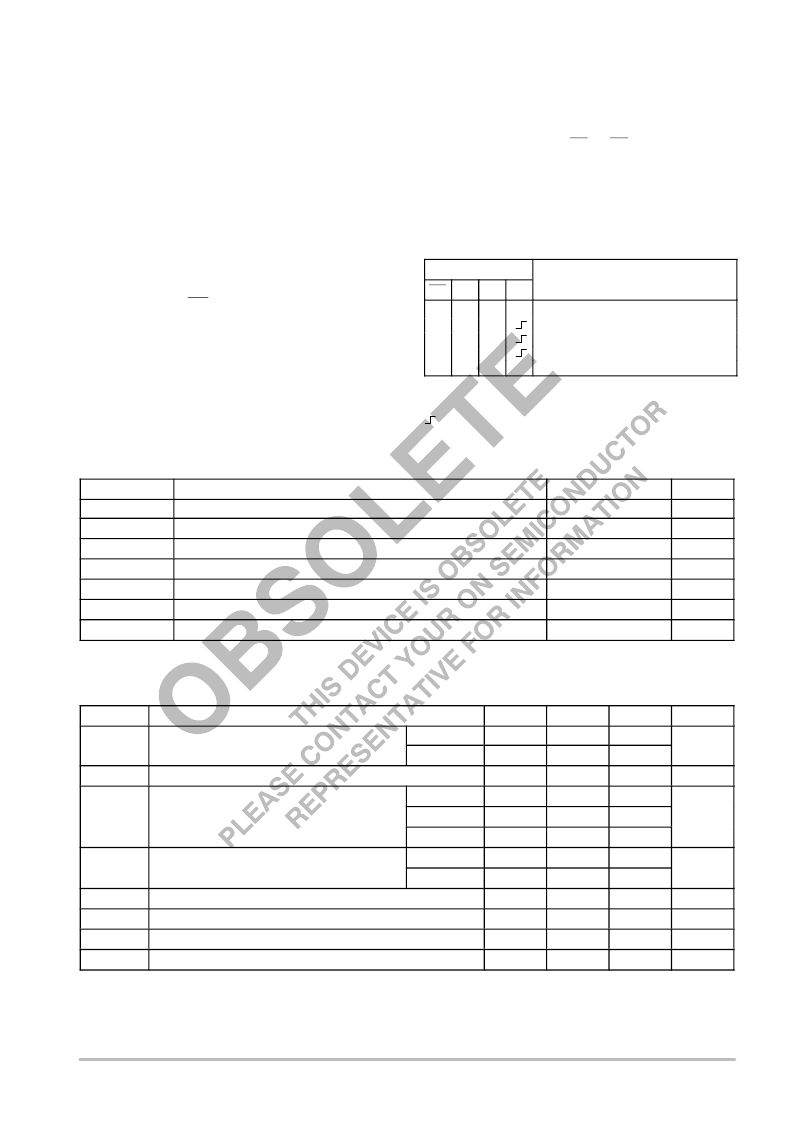
TRUTH TABLE
Inputs
Response
MR
S
1
S
0
CP
L
H
H
H
H
X
H
L
H
L
X
H
H
L
L
X
Asynchronous Reset; Q
0
Q
7
= LOW
Parallel Load; I/O
n
→
Q
n
Shift Rights; DS
0
→
Q
0
, Q
0
→
Q
1
, etc.
Shift Left; DS
7
→
Q
7
, Q
7
→
Q
6
, etc.
Hold
X
H = HIGH Voltage Level
L = LOW Voltage Level
X = Immaterial
= LOW-to-HIGH Transition
MAXIMUM RATINGS*
Symbol
Parameter
Value
Unit
V
CC
V
IN
DC Supply Voltage (Referenced to GND)
0.5 to +7.0
V
DC Input Voltage (Referenced to GND)
0.5 to V
CC
+0.5
V
V
OUT
DC Output Voltage (Referenced to GND)
0.5 to V
CC
+0.5
V
I
IN
DC Input Current, per Pin
±
20
mA
I
OUT
DC Output Sink/Source Current, per Pin
±
50
mA
I
CC
DC V
CC
or GND Current per Output Pin
±
50
mA
T
stg
Storage Temperature
65 to +150
°
C
*Maximum Ratings are those values beyond which damage to the device may occur. Functional operation should be restricted to the
Recommended Operating Conditions.
RECOMMENDED OPERATING CONDITIONS
Symbol
Parameter
Min
Typ
Max
Unit
V
CC
Supply Voltage
′
AC
2.0
5.0
6.0
V
′
ACT
4.5
5.0
5.5
V
IN
, V
OUT
DC Input Voltage, Output Voltage (Ref. to GND)
0
V
CC
V
t
r
, t
f
Input Rise and Fall Time (Note 1)
′
AC Devices except Schmitt Inputs
V
CC
@ 3.0 V
150
V
CC
@ 4.5 V
40
ns/V
V
CC
@ 5.5 V
25
t
r
, t
f
Input Rise and Fall Time (Note 2)
′
ACT Devices except Schmitt Inputs
V
CC
@ 4.5 V
10
ns/V
V
CC
@ 5.5 V
8.0
T
J
Junction Temperature (PDIP)
140
°
C
T
A
Operating Ambient Temperature Range
40
25
85
°
C
I
OH
Output Current
High
24
mA
I
OL
Output Current
Low
24
mA
1. V
IN
from 30% to 70% V
CC
; see individual Data Sheets for devices that differ from the typical input rise and fall times.
2. V
IN
from 0.8 V to 2.0 V; see individual Data Sheets for devices that differ from the typical input rise and fall times.
相關(guān)PDF資料 |
PDF描述 |
|---|---|
| MC74ACT299DW | 8−Input Universal Shift/Storage Register with Common Parallel I/O Pins |
| MC74ACT299DWR2 | 8−Input Universal Shift/Storage Register with Common Parallel I/O Pins |
| MC74ACT299N | 8−Input Universal Shift/Storage Register with Common Parallel I/O Pins |
| MC74AC32DG | QUAD 2-INPUT OR GATE |
| MC74AC32DR2 | QUAD 2-INPUT OR GATE |
相關(guān)代理商/技術(shù)參數(shù) |
參數(shù)描述 |
|---|---|
| MC74AC32 | 制造商:ONSEMI 制造商全稱:ON Semiconductor 功能描述:QUAD 2-INPUT OR GATE |
| MC74AC32/D | 制造商:ONSEMI 制造商全稱:ON Semiconductor 功能描述:QUAD 2-INPUT OR GATE |
| MC74AC323 | 制造商:ONSEMI 制造商全稱:ON Semiconductor 功能描述:8-INPUT UNIVERSAL SHIFT/ STORAGE REGISTER WITH SYNCHRONOUS RESET AND COMMON I/O PINS |
| MC74AC323DW | 制造商:MOTOROLA 制造商全稱:Motorola, Inc 功能描述:8-INPUT UNIVERSAL SHIFT/ STORAGE REGISTER WITH SYNCHRONOUS RESET AND COMMON I/O PINS |
| MC74AC323N | 制造商:MOTOROLA 制造商全稱:Motorola, Inc 功能描述:8-INPUT UNIVERSAL SHIFT/ STORAGE REGISTER WITH SYNCHRONOUS RESET AND COMMON I/O PINS |
發(fā)布緊急采購(gòu),3分鐘左右您將得到回復(fù)。