- 您現(xiàn)在的位置:買賣IC網(wǎng) > PDF目錄383560 > MC74A5-50T (ON SEMICONDUCTOR) RELAY SWITCH; SMA RELAY SWITCH; FREQUENCY RANGE: DC-18 GHz; SWICH TYPE: TRANSFER; FEATURE: INDICATORS, LATCHING & SELF CUT OFF; ACTUATING VOLTAGE: 28; VSWR: 1.50:1 @ 18 GHz PDF資料下載
參數(shù)資料
| 型號: | MC74A5-50T |
| 廠商: | ON SEMICONDUCTOR |
| 英文描述: | RELAY SWITCH; SMA RELAY SWITCH; FREQUENCY RANGE: DC-18 GHz; SWICH TYPE: TRANSFER; FEATURE: INDICATORS, LATCHING & SELF CUT OFF; ACTUATING VOLTAGE: 28; VSWR: 1.50:1 @ 18 GHz |
| 中文描述: | 串行數(shù)字溫度傳感器 |
| 文件頁數(shù): | 5/12頁 |
| 文件大小: | 122K |
| 代理商: | MC74A5-50T |
MC74
http://onsemi.com
5
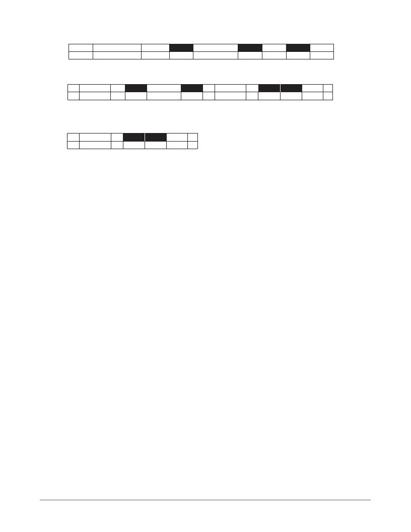
Figure 1. SMBus Protocols
DATA
8 Bits
Data Byte: reads from
the register set by the
command byte.
S
ADDRESS
7 Bits
Slave Address
WR
ACK
COMMAND
8 Bits
Command Byte: selects
which register you are
writing to.
DATA
8 Bits
P
ACK
ACK
S
ADDRESS
7 Bits
Slave Address
WR
ACK
COMMAND
8 Bits
Command Byte: selects
which register you are
reading from.
RD
NACK
S
ADDRESS
7 Bits
Slave Address: repeated
due to change in data–
flow direction.
ACK
ACK
P
DATA
8 Bits
RD
NACK
S
ADDRESS
7 Bits
ACK
P
Data Byte: data goes
into the register set
by the command byte.
Data Byte: reads data from
the register commanded by
the last Read Byte.
S = Start Condition
P = Stop Condition
Shaded = Slave Transmission
Write Byte Format
Read Byte Format
Receive Byte Format
Start Condition (START)
The MC74 continuously monitors the SDA and SCL lines
for a start condition (a HIGH to LOW transition of SDA
while SCL is HIGH) and will not respond until this condition
is met.
Address Byte
Immediately following the Start Condition, the host must
transmit the address byte to the MC74. The states of A1 and
A0 determine the 7–bit SMBus address for the MC74. The
7–bit address transmitted in the serial bit stream must match
for the MC74 to respond with an Acknowledge (indicating
the MC74 is on the bus and ready to accept data). The eighth
bit in the Address Byte is a Read–Write Bit. This bit is a 1
for a read operation or 0 for a write operation. During the
first phase of any transfer this bit will be set = 0 to indicate
that the command byte is being written.
Acknowledge (ACK)
Acknowledge (ACK) provides a positive handshake
between the host and the MC74. The host releases SDA after
transmitting eight bits, then generates a ninth clock cycle to
allow the MC74 to pull the SDA line LOW to acknowledge
that it successfully received the previous eight bits of data or
address.
Data Byte
After a successful ACK of the address byte, the host must
transmit the data byte to be written or clock out the data to
be read. (See the appropriate timing diagrams. ) ACK will
be generated after a successful write of a data byte into the
MC74.
Stop Condition (STOP)
Communications must be terminated by a stop condition
(a LOW to HIGH transition of SDA while SCL is HIGH).
The Stop Condition must be communicated by the
transmitter to the MC74. NOTE:
Refer to Timing Diagrams
for serial bus timing.
相關(guān)PDF資料 |
PDF描述 |
|---|---|
| MC74AC08MEL | QUAD 2-INPUT AND GATE |
| MC74ACT08DR2 | QUAD 2-INPUT AND GATE |
| MC74ACT08DTR2G | QUAD 2-INPUT AND GATE |
| MC74ACT08MEL | QUAD 2-INPUT AND GATE |
| MC74ACT08NG | QUAD 2-INPUT AND GATE |
相關(guān)代理商/技術(shù)參數(shù) |
參數(shù)描述 |
|---|---|
| MC74AC00 | 制造商:ONSEMI 制造商全稱:ON Semiconductor 功能描述:QUAD 2-INPUT NAND GATE |
| MC74AC00D | 功能描述:邏輯門 2-6V Quad 2-Input RoHS:否 制造商:Texas Instruments 產(chǎn)品:OR 邏輯系列:LVC 柵極數(shù)量:2 線路數(shù)量(輸入/輸出):2 / 1 高電平輸出電流:- 16 mA 低電平輸出電流:16 mA 傳播延遲時間:3.8 ns 電源電壓-最大:5.5 V 電源電壓-最小:1.65 V 最大工作溫度:+ 125 C 安裝風(fēng)格:SMD/SMT 封裝 / 箱體:DCU-8 封裝:Reel |
| MC74AC00DG | 功能描述:邏輯門 2-6V Quad 2-Input NAND RoHS:否 制造商:Texas Instruments 產(chǎn)品:OR 邏輯系列:LVC 柵極數(shù)量:2 線路數(shù)量(輸入/輸出):2 / 1 高電平輸出電流:- 16 mA 低電平輸出電流:16 mA 傳播延遲時間:3.8 ns 電源電壓-最大:5.5 V 電源電壓-最小:1.65 V 最大工作溫度:+ 125 C 安裝風(fēng)格:SMD/SMT 封裝 / 箱體:DCU-8 封裝:Reel |
| MC74AC00DR2 | 功能描述:邏輯門 2-6V Quad 2-Input RoHS:否 制造商:Texas Instruments 產(chǎn)品:OR 邏輯系列:LVC 柵極數(shù)量:2 線路數(shù)量(輸入/輸出):2 / 1 高電平輸出電流:- 16 mA 低電平輸出電流:16 mA 傳播延遲時間:3.8 ns 電源電壓-最大:5.5 V 電源電壓-最小:1.65 V 最大工作溫度:+ 125 C 安裝風(fēng)格:SMD/SMT 封裝 / 箱體:DCU-8 封裝:Reel |
| MC74AC00DR2G | 功能描述:邏輯門 2-6V Quad 2-Input NAND RoHS:否 制造商:Texas Instruments 產(chǎn)品:OR 邏輯系列:LVC 柵極數(shù)量:2 線路數(shù)量(輸入/輸出):2 / 1 高電平輸出電流:- 16 mA 低電平輸出電流:16 mA 傳播延遲時間:3.8 ns 電源電壓-最大:5.5 V 電源電壓-最小:1.65 V 最大工作溫度:+ 125 C 安裝風(fēng)格:SMD/SMT 封裝 / 箱體:DCU-8 封裝:Reel |
發(fā)布緊急采購,3分鐘左右您將得到回復(fù)。