- 您現(xiàn)在的位置:買賣IC網(wǎng) > PDF目錄382306 > MC44608P75 (ON SEMICONDUCTOR) Few External Components Reliable Flexible GreenLine Very High Voltage PWM Controller PDF資料下載
參數(shù)資料
| 型號(hào): | MC44608P75 |
| 廠商: | ON SEMICONDUCTOR |
| 元件分類: | 穩(wěn)壓器 |
| 英文描述: | Few External Components Reliable Flexible GreenLine Very High Voltage PWM Controller |
| 中文描述: | SWITCHING CONTROLLER, 82 kHz SWITCHING FREQ-MAX, PDIP8 |
| 封裝: | PLASTIC, DIP-8 |
| 文件頁(yè)數(shù): | 7/16頁(yè) |
| 文件大小: | 266K |
| 代理商: | MC44608P75 |
第1頁(yè)第2頁(yè)第3頁(yè)第4頁(yè)第5頁(yè)第6頁(yè)當(dāng)前第7頁(yè)第8頁(yè)第9頁(yè)第10頁(yè)第11頁(yè)第12頁(yè)第13頁(yè)第14頁(yè)第15頁(yè)第16頁(yè)

MC44608
http://onsemi.com
7
Figure 5.
Vcont
2.4 V
Iprim
DMG
Clock
OSC
4 V
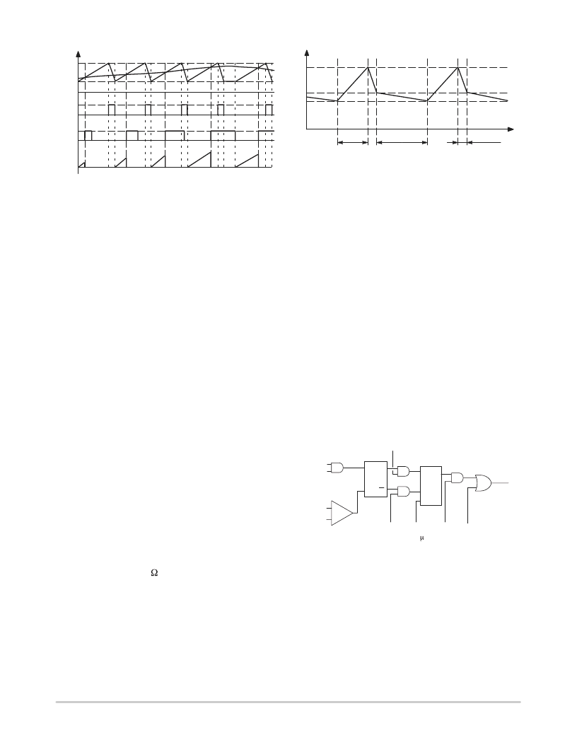
The OSC and Clock signals are provided according to the
Figure 5. The Clock signals correspond to the CT capacitor
discharge. The bottom curve represents the current flowing
in the sense resistor Rcs. It starts from zero and stops when
the sawtooth value is equal to the control voltage Vcont. In
this way the SMPS is regulated with a voltage mode control.
Overvoltage Protection
The MC44608 offers two OVP functions:
– a fixed function that detects when VCC is higher than
15.4V
– a programmable function that uses the demag pin. The
current flowing into the demag pin is mirrored and
compared to the reference current Iovp (120
μ
A). Thus this
OVP is quicker as it is not impacted by the VCC inertia and
is called QOVP.
In both cases, once an OVP condition is detected, the
output is latched off until a new circuit START–UP.
Start–up Management
The Vi pin 8 is directly connected to the HV DC rail Vin.
This high voltage current source is internally connected to
the VCC pin and thus is used to charge the VCC capacitor. The
VCC capacitor charge period corresponds to the Start–up
phase. When the VCC voltage reaches 13V, the high voltage
9mA current source is disabled and the device starts
working. The device enters into the switching phase.
It is to be noticed that the maximum rating of the Vi pin 8
is 700V. ESD protection circuitry is not currently added to
this pin due to size limitations and technology constraints.
Protection is limited by the drain–substrate junction in
avalanche breakdown. To help increase the application
safety against high voltage spike on that pin it is possible to
insert a small wattage 1k series resistor between the Vin
rail and pin 8.
The Figure 6 shows the VCC voltage evolution in case of
no external current source providing current into the VCC
pin during the switching phase. This case can be
encountered in SMPS when the self supply through an
auxiliary winding is not present (strong overload on the
SMPS output for example). The Figure 16 also depicts this
working configuration.
Figure 6. Hiccup Mode
Start–up
Phase
Latched off
Phase
Switching
Phase
VCC
6.5 V
10 V
13 V
In case of the hiccup mode, the duty cycle of the switching
phase is in the range of 10%.
Mode Transition
The LW latch Figure 7 is the memory of the working status
at the end of every switching sequence.
Two different cases must be considered for the logic at the
termination of the SWITCHING PHASE:
1. No Over Current was observed
2. An Over Current was observed
These 2 cases are corresponding to the signal labelled
NOC in case of “No Over Current” and “OC” in case of Over
Current. So the effective working status at the end of the ON
time memorized in LW corresponds to Q=1 for no over
current and Q=0 for over current.
This sequence is repeated during the Switching phase.
Several events can occur:
1. SMPS switch OFF
2. SMPS output overload
3. Transition from Normal to Pulsed Mode
4. Transition from Pulsed Mode to Normal Mode
Figure 7. Transition Logic
&
I
demag
S
Q
R
LW
+
–
&
CS
Q
&
R2
Q
S
Mode
R1
LEB out
1 V
VPWM
OUT
Stand–by
Start–up
Phase
Switching
Phase
Start–up
Phase
NOC
OC
> 24 A
Latched Off
Phase
&
S1
Switch
1. SMPS SWITCH OFF
When the mains is switched OFF, so long as the bulk
electrolithic bulk capacitor provides energy to the SMPS,
the controller remains in the switching phase. Then the peak
current reaches its maximum peak value, the switching
frequency decreases and all the secondary voltages are
reduced. The VCC voltage is also reduced. When VCC is
equal to 10V, the SMPS stops working.
相關(guān)PDF資料 |
PDF描述 |
|---|---|
| MC44608 | Few External Components Reliable Flexible GreenLine Very High Voltage PWM Controller |
| MC44608P40 | RW-S Series - Econoline Regulated DC-DC Converters; Input Voltage (Vdc): 05V; Output Voltage (Vdc): 09V; Power: 2W; DIP24 Low Profile Miniature Package; 1kVDC Isolation; Feedback Regulated Output; 2:1 Wide Range Voltage Input; Continuous Short Circuit Protection; Less than 7mm Height; SMD Pinning Option; Efficiency to 87% |
| MC44C401 | MTS Stereo Encoder |
| MC44C401FA | MTS Stereo Encoder |
| MC4741C | DIFFERENTIAL INPUT OPERATIONAL AMPLIFIER |
相關(guān)代理商/技術(shù)參數(shù) |
參數(shù)描述 |
|---|---|
| MC44608P75G | 功能描述:電壓模式 PWM 控制器 75KHz High Voltage SMPS PWM RoHS:否 制造商:Texas Instruments 輸出端數(shù)量:1 拓?fù)浣Y(jié)構(gòu):Buck 輸出電壓:34 V 輸出電流: 開關(guān)頻率: 工作電源電壓:4.5 V to 5.5 V 電源電流:600 uA 最大工作溫度:+ 125 C 最小工作溫度:- 40 C 封裝 / 箱體:WSON-8 封裝:Reel |
| MC4466 | 制造商:SHENZHENFREESCALE 制造商全稱:ShenZhen FreesCale Electronics. Co., Ltd 功能描述:N-Channel 30-V (D-S) MOSFET High performance trench technology |
| MC4468 | 制造商:SHENZHENFREESCALE 制造商全稱:ShenZhen FreesCale Electronics. Co., Ltd 功能描述:N-Channel 30-V (D-S) MOSFET High performance trench technology |
| MC44722A | 制造商:MOTOROLA 制造商全稱:Motorola, Inc 功能描述:Advanced Digital Video Encoder |
| MC44722AVFU | 制造商:Rochester Electronics LLC 功能描述: 制造商:Freescale Semiconductor 功能描述: |
發(fā)布緊急采購(gòu),3分鐘左右您將得到回復(fù)。