- 您現(xiàn)在的位置:買賣IC網(wǎng) > PDF目錄371036 > MC44302AP (MOTOROLA INC) ADVANCED MULTI-STANDARD VIDEO/SOUND IF PDF資料下載
參數(shù)資料
| 型號: | MC44302AP |
| 廠商: | MOTOROLA INC |
| 元件分類: | 消費家電 |
| 英文描述: | ADVANCED MULTI-STANDARD VIDEO/SOUND IF |
| 中文描述: | SPECIALTY CONSUMER CIRCUIT, PDIP28 |
| 封裝: | PLASTIC, DIP-28 |
| 文件頁數(shù): | 4/28頁 |
| 文件大小: | 612K |
| 代理商: | MC44302AP |
第1頁第2頁第3頁當前第4頁第5頁第6頁第7頁第8頁第9頁第10頁第11頁第12頁第13頁第14頁第15頁第16頁第17頁第18頁第19頁第20頁第21頁第22頁第23頁第24頁第25頁第26頁第27頁第28頁
MC44302A
4
MOTOROLA ANALOG IC DEVICE DATA
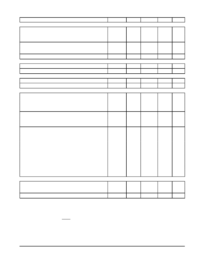
ELECTRICAL CHARACTERISTICS
(continued)
(VCC = 5.0 V, TA = 25
°
C.)
Characteristic
Unit
Max
Typ
Min
Symbol
PHASE–LOCKED LOOP
Acquisition Circuit Filter Voltage (Pin 18)
Unlocked with No–Signal
Unlocked to Locked Sweep Range upon Signal Acquisition
Locked, Final Static Condition
VPLL(Acq)
V
–
–
–
2.7
–
–
–
1.2 to 4.3
4.3
VCO Filter Voltage (Pin 19)
Unlocked
Locked, Final Static Condition
VPLL(VCO)
V
–
–
3.2
3.2
–
–
Video IF Lock–Up Time
tIF(lock)
–
5.0
–
ms
HORIZONTAL GATING SYSTEM
Sync Separator Input Threshold Voltage (Pin 17)
Vth(Sync)
VPLL(Horiz)
–
3.4
–
V
PLL Filter Voltage, Locked or Unlocked with No–Signal (Pin 16)
–
2.9
±
1.1
–
V
RF AGC
RF AGC Delay Voltage Range (Pin 15)
VAGC(DLY)
IO(sink)
–
1.7 to 2.4
–
V
RF AGC Output Current (Pin 13)
1.0
2.0
–
mA
LOGIC CONTROL
Mode Select Voltage Range (Pin 10)
PAL 1
PAL 2
SECAM
NTSC
Vth(Mode)
V
4.7 to 5.0
3.5 to 4.1
2.3 to 2.9
0 to 0.3
4.6 to 5.0
3.4 to 4.2
2.2 to 3.0
0 to 0.4
–
–
–
–
AFT Switch Threshold (Pin 12)
AFT Output, Pin 11, Sourcing when IF Frequency is Low
AFT Output, Pin 11, Sinking when IF Frequency is Low
AFT Output, Pin 11, Disabled (Note 8)
Vth(AFT)
–
–
–
5.0
0
2.5
–
–
–
Audio Switch/Video Invert Voltage Range (Pin 3)
Audio 1, Internal Audio (AM or FM) appears at Pins 24 and 27,
Positive Video appears at Pin 6,
Negative Video appears at Pin 5
Audio 2, Internal Audio (AM or FM) appears at Pin 24,
External Audio appears at Pin 27,
Positive Video appears at Pin 6,
Negative Video appears at Pin 5
Video 1, Internal Audio (AM or FM) appears at Pins 24 and 27,
Positive Video appears at Pin 6,
Negative Video appears at Pin 5
Video 2, Internal Audio (AM or FM) appears at Pins 24 and 27,
Positive Video appears at Pin 5,
Negative Video appears at Pin 6
Vth(AS/VI)
V
3.4 to 5.0
3.3 to 5.0
–
1.8 to 2.2
1.7 to 2.3
–
0.6 to 0.9
0.5 to 1.0
–
0 to 0.2
0 to 0.3
–
TOTAL DEVICE
Operating Voltage
TA = 25
°
C
TA = 0
°
C to 70
°
C
Power Supply Current (VCC = 5.0 V)
VCC
V
4.5
4.75
5.0
–
5.5
5.5
ICC
–
100
–
mA
NOTES:
1.
Vin = 1.0 mVrms signal at 45.75 MHz with 75% modulated staircase at 3.58 MHz.
2.Vin = 100
μ
Vrms signal at 41.25 MHz added to signal in Note 1.
3.Differential carrier level at video IF inputs to cause the negative detector output to go positive by 0.1 V from ground.
4.FM Modulation =
±
25 kHz deviation at 1.0 kHz for 4.5 MHz intercarrier.
±
50 kHz deviation at 1.0 kHz for 5.5 MHz intercarrier.
5.AM Modulation = 30% depth at 1.0 kHz for 4.5 MHz and 5.5 MHz intercarrier.
VO(FM)
VO(AM)
6.AM Rejection (dB) = 20 log
7.Tested with 15
μ
H sound quadrature coil in parallel with 68 pF and 10 k
.
8.The AFT output can be disabled by leaving Pin 12 disconnected or by biasing it to the voltage level shown above. When disabled, the output will be
internally clamped to one half of VCC.
相關PDF資料 |
PDF描述 |
|---|---|
| MC44353DTB | MULTI.STANDARD AND PAL/NTSC MODULATOR ICs |
| MC44353 | MULTI.STANDARD AND PAL/NTSC MODULATOR ICs |
| MC44355DTB | MULTI.STANDARD AND PAL/NTSC MODULATOR ICs |
| MC44354DTB | MULTI.STANDARD AND PAL/NTSC MODULATOR ICs |
| MC44354DW | MULTI.STANDARD AND PAL/NTSC MODULATOR ICs |
相關代理商/技術參數(shù) |
參數(shù)描述 |
|---|---|
| MC4433 | 制造商:SHENZHENFREESCALE 制造商全稱:ShenZhen FreesCale Electronics. Co., Ltd 功能描述:P-Channel 30-V (D-S) MOSFET Fast switching speed |
| MC4435 | 制造商:SHENZHENFREESCALE 制造商全稱:ShenZhen FreesCale Electronics. Co., Ltd 功能描述:P-Channel 30-V (D-S) MOSFET Fast switching speed |
| MC44353 | 制造商:MOTOROLA 制造商全稱:Motorola, Inc 功能描述:MULTI.STANDARD AND PAL/NTSC MODULATOR ICs |
| MC44353DTB | 制造商:MOTOROLA 制造商全稱:Motorola, Inc 功能描述:MULTI.STANDARD AND PAL/NTSC MODULATOR ICs |
| MC44353DW | 制造商:MOTOROLA 制造商全稱:Motorola, Inc 功能描述:MULTI.STANDARD AND PAL/NTSC MODULATOR ICs |
發(fā)布緊急采購,3分鐘左右您將得到回復。