- 您現(xiàn)在的位置:買賣IC網(wǎng) > PDF目錄371022 > MC33110 (Motorola, Inc.) LOW VOLTAGE COMPANDER PDF資料下載
參數(shù)資料
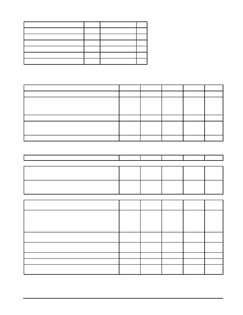
| 型號: | MC33110 |
| 廠商: | Motorola, Inc. |
| 英文描述: | LOW VOLTAGE COMPANDER |
| 中文描述: | 低電壓擴(kuò)展器 |
| 文件頁數(shù): | 3/13頁 |
| 文件大小: | 205K |
| 代理商: | MC33110 |
MC33110
3
MOTOROLA RF/IF DEVICE DATA
áááááááááááááááááááá
áááááááááááááááááááá
áááááááááááááááááááá
Conditions” table provides conditions for actual device operation.
2.ESD data available upon request.
áááááááááááááááááááá
áááááááááááááááááááá
áááááááááááááááááááá
áááááááááááááááááááá
áááááááááááááááááááá
RECOMMENDED OPERATING CONDITIONS
Characteristic
Symbol
Min
Typ
Max
Unit
VCC Supply Voltage
Input Voltage Range
Compressor, 2.1 V < VCC < 7.0 V
Expander, VCC = 2.1 V
Expander, 3.0 V < VCC < 7.0 V
Input Frequency
VCC
VIR
2.1
–
7.0
Vdc
0
0
0
–
–
–
1.0
0.25
0.316
Vrms
Fin
RL
100
–
20 k
Hz
Output Load
Compressor (Pin 11, VO = 100 mV)
Expander (Pin 4, VO = 100 mV)
300
150
–
–
∞
∞
Ambient Temperature
TA
–40
–
85
°
C
All limits are not necessarily functional concurrently.
ELECTRICAL CHARACTERISTICS
(VCC = 5.0 V, f = 1.0 kHz, unless otherwise noted, TA = 25
°
C, see Figure 1)
Characteristic
POWER SUPPLY
Symbol
Min
Typ
Max
Unit
Power Supply Current
VCC = 5.0 V
VCC = 2.1 V
VB Voltage
VCC = 5.0 V
2.1 V < VCC < 7.0 V
COMPRESSOR
ICC
–
–
3.5
3.3
5.5
–
mA
VB
2.4
–
2.5
VCC/2
2.6
–
Vdc
0 dB Gain
Vin = 100 mVrms, Pin 1 = Open
G(CO)
–1.5
0
1.5
dB
Gain Tracking
@ Vin = 1.0 Vrms, output relative to G(CO)
@ Vin = 10 mVrms, output relative to G(CO)
@ Vin = 1.0 mVrms, output relative to G(CO)
@ Vin = 100
μ
Vrms, output relative to G(CO)
Gt
9.0
–
–
–31
10
–10
–20
–30
11
–
–
–29
dB
Total Harmonic Distortion
Vin = 100 mVrms, f = 1.0 kHz
THD
0
0.1
1.5
%
Power Supply Rejection
f = 1.0 kHz, CVB = 10
μ
F, Vin = – 20 dB
Attack Time (Capacitor @ Pin 12 = 2.2
μ
F)
PSRR
–
22
–
dB
ta(C)
td(C)
Rin
–
6.0
–
ms
Decay Time (Capacitor @ Pin 12 = 2.2
μ
F)
–
20
–
ms
Input Impedance
Pin 10
Pin 8
–
–
10
3.2
–
–
k
相關(guān)PDF資料 |
PDF描述 |
|---|---|
| MC33110P | ECONOLINE: RSZ/P - 1kVDC |
| MC33111D | LOW VOLTAGE COMPANDER |
| MC33111P | ECONOLINE: RSZ/P - 1kVDC |
| MC33111 | Low Voltage Compander |
| MC33128D | POWER MANAGEMENT CONTROLLER |
相關(guān)代理商/技術(shù)參數(shù) |
參數(shù)描述 |
|---|---|
| MC33110D | 制造商:MOTOROLA 制造商全稱:Motorola, Inc 功能描述:LOW VOLTAGE COMPANDER |
| MC33110P | 制造商:MOTOROLA 制造商全稱:Motorola, Inc 功能描述:LOW VOLTAGE COMPANDER |
| MC33111 | 制造商:FREESCALE 制造商全稱:Freescale Semiconductor, Inc 功能描述:Low Voltage Compander |
| MC33111D | 制造商:FREESCALE 制造商全稱:Freescale Semiconductor, Inc 功能描述:Low Voltage Compander |
| MC33111P | 制造商:MOTOROLA 制造商全稱:Motorola, Inc 功能描述:LOW VOLTAGE COMPANDER |
發(fā)布緊急采購,3分鐘左右您將得到回復(fù)。