- 您現(xiàn)在的位置:買賣IC網(wǎng) > PDF目錄371022 > MC33102D (MOTOROLA INC) DUAL SLEEP-MODE OPERATIONAL AMPLIFIER PDF資料下載
參數(shù)資料
| 型號: | MC33102D |
| 廠商: | MOTOROLA INC |
| 元件分類: | 運動控制電子 |
| 英文描述: | DUAL SLEEP-MODE OPERATIONAL AMPLIFIER |
| 中文描述: | DUAL OP-AMP, 3000 uV OFFSET-MAX, 4.6 MHz BAND WIDTH, PDSO8 |
| 封裝: | PLASTIC, SO-8 |
| 文件頁數(shù): | 11/14頁 |
| 文件大小: | 300K |
| 代理商: | MC33102D |
MC33102
11
MOTOROLA ANALOG IC DEVICE DATA
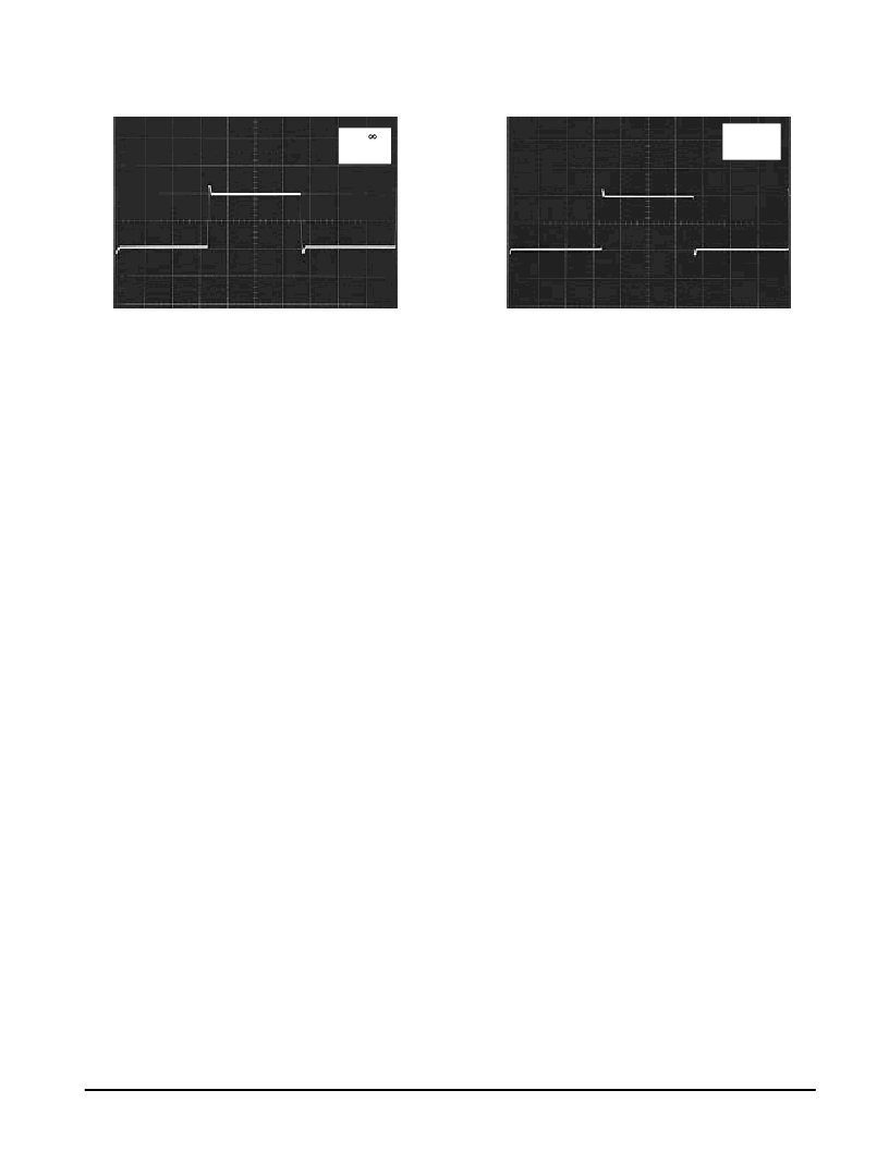
t, TIME (50
μ
s/DIV)
,
P
V
t, TIME (50
μ
s/DIV)
RL = 600
CL = 0 pF
,
P
V
RL =
CL = 0 pF
Figure 37. Sleepmode Small Signal
Transient Response
Figure 38. Awakemode Small Signal
Transient Response
CIRCUIT INFORMATION
The MC33102 was designed primarily for applications
where high performance (which requires higher current drain)
is required only part of the time. The two–state feature of this
op amp enables it to conserve power during idle times, yet be
powered up and ready for an input signal. Possible
applications include laptop computers, automotive, cordless
phones, baby monitors, and battery operated test equipment.
Although most applications will require low power
consumption, this device can be used in any application
where better efficiency and higher performance is needed.
The Sleep–Mode
amplifier has two states; a sleepmode
and an awakemode. In the sleepmode state, the amplifier is
active and functions as a typical micropower op amp. When a
signal is applied to the amplifier causing it to source or sink
sufficient current (see Figure 13), the amplifier will
automatically switch to the awakemode. See Figures 20 and
21 for transition times with 600
and 10 k
loads.
The awakemode uses higher drain current to provide a
high slew rate, gain bandwidth, and output current capability.
In the awakemode, this amplifier can drive 27 Vpp into a
600
load with VS =
±
15 V.
An internal delay circuit is used to prevent the amplifier
from returning to the sleepmode at every zero crossing. This
delay circuit also eliminates the crossover distortion
commonly found in micropower amplifiers. This amplifier can
process frequencies as low as 1.0 Hz without the amplifier
returning to sleepmode, depending on the load.
The first stage PNP differential amplifier provides low noise
performance in both the sleep and awake modes, and an all
NPN output stage provides symmetrical source and sink AC
frequency response.
APPLICATIONS INFORMATION
The MC33102 will begin to function at power supply
voltages as low as VS =
±
1.0 V at room temperature. (At this
voltage, the output voltage swing will be limited to a few
hundred millivolts.) The input voltages must range between
VCC and VEE supply voltages as shown in the maximum
rating table. Specifically,
allowing the input to go more
negative than 0.3 V below VEE may cause product
damage.
Also, exceeding the input common mode voltage
range on either input may cause phase reversal, even if the
inputs are between VCC and VEE.
When power is initially applied, the part may start to
operate in the awakemode. This is because of the currents
generated due to charging of internal capacitors. When this
occurs and the sleepmode state is desired, the user will have
to wait approximately 1.5 seconds before the device will
switch back to the sleepmode. To prevent this from occurring,
ramp the power supplies from 1.0 V to full supply. Notice that
the device is more prone to switch into the awakemode when
VEE is adjusted than with a similar change in VCC.
The amplifier is designed to switch from sleepmode to
awakemode whenever the output current exceeds a preset
current threshold (ITH) of approximately 160
μ
A. As a result,
the output switching threshold voltage (VST) is controlled by
the output loading resistance (RL). This loading can be a load
resistor, feedback resistors, or both. Then:
VST = (160
μ
A)
×
RL
Large valued load resistors require a large output voltage
to switch, but reduce unwanted transitions to the
awakemode. For instance, in cases where the amplifier is
connected with a large closed loop gain (ACL), the input offset
voltage (VIO) is multiplied by the gain at the output and could
produce an output voltage exceeding VST with no input
signal applied.
Small values of RL allow rapid transition to the awakemode
because most of the transition time is consumed slewing in
the sleepmode until VST is reached (see Figures 20, 21). The
output switching threshold voltage VST is higher for larger
values of RL, requiring the amplifier to slew longer in the
slower sleepmode state before switching to the awakemode.
相關(guān)PDF資料 |
PDF描述 |
|---|---|
| MC33102P | DUAL SLEEP-MODE OPERATIONAL AMPLIFIER |
| MC33110D | LOW VOLTAGE COMPANDER |
| MC33110 | LOW VOLTAGE COMPANDER |
| MC33110P | ECONOLINE: RSZ/P - 1kVDC |
| MC33111D | LOW VOLTAGE COMPANDER |
相關(guān)代理商/技術(shù)參數(shù) |
參數(shù)描述 |
|---|---|
| MC33102P | 制造商:Motorola Inc 功能描述: 制造商:ON Semiconductor 功能描述: 制造商:MOTOROLA 功能描述: |
| MC33110 | 制造商:MOTOROLA 制造商全稱:Motorola, Inc 功能描述:LOW VOLTAGE COMPANDER |
| MC33110D | 制造商:MOTOROLA 制造商全稱:Motorola, Inc 功能描述:LOW VOLTAGE COMPANDER |
| MC33110P | 制造商:MOTOROLA 制造商全稱:Motorola, Inc 功能描述:LOW VOLTAGE COMPANDER |
| MC33111 | 制造商:FREESCALE 制造商全稱:Freescale Semiconductor, Inc 功能描述:Low Voltage Compander |
發(fā)布緊急采購,3分鐘左右您將得到回復(fù)。