- 您現(xiàn)在的位置:買賣IC網(wǎng) > PDF目錄11745 > MC100EP446MNR4G (ON Semiconductor)IC CONV PAR/SER 8BIT DIFF 32-QFN PDF資料下載
參數(shù)資料
| 型號(hào): | MC100EP446MNR4G |
| 廠商: | ON Semiconductor |
| 文件頁數(shù): | 8/20頁 |
| 文件大小: | 0K |
| 描述: | IC CONV PAR/SER 8BIT DIFF 32-QFN |
| 標(biāo)準(zhǔn)包裝: | 1,000 |
| 應(yīng)用: | 數(shù)據(jù)管理 |
| 接口: | 差分 |
| 電源電壓: | 3 V ~ 5.5 V |
| 封裝/外殼: | 32-VFQFN 裸露焊盤 |
| 供應(yīng)商設(shè)備封裝: | 32-QFN(5x5) |
| 包裝: | 帶卷 (TR) |
| 安裝類型: | 表面貼裝 |
MC10EP446, MC100EP446
http://onsemi.com
16
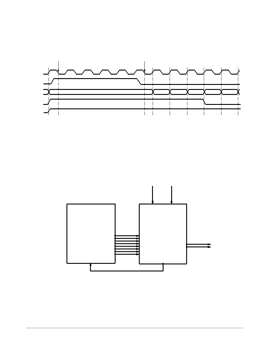
The differential synchronous CKEN inputs (Pins 6 and 7), disable the internal clock circuitry. The synchronous CKEN will
suspend all of the device activities and prevent runt pulses from being generated. The rising edge of CKEN followed by the
falling edge of CLK will suspend all activities. The falling edge of CKEN followed by the falling edge of CLK will resume
all activities (Figure 13).
Figure 13. Timing Diagram with CKEN with CKSEL HIGH
CLK
CKEN
SOUT
CKSEL
D11
D01D21D31
PCLK
D41D51
Internal Clock
Disabled
Internal Clock
Enabled
The differential PCLK output (Pins 14 and 15) is a word
framer and can help the user synchronize the serial data
output, SOUT (Pins 11 and 12), in their applications.
Furthermore, PCLK can be used as a trigger for input
parallel data (Figure 14).
An internally generated voltage supply, the VBB pin, is
available to this device only. For single–ended input
conditions, the unused differential input is connected to VBB
as a switching reference voltage. VBB may also rebias AC
coupled inputs. When used, decouple VBB and VCC via a
0.01
mF capacitor and limit current sourcing or sinking to
0.5 mA. When not used, VBB should be left open. Also, both
outputs of the differential pair must be terminated (50
W to
VTT) even if only one output is used.
Figure 14. PCLK as Trigger Application
TRIGGER
Pattern Generator
Data Format Logic
(FPGA, ASIC)
PARALLEL
DA
TA
OUTPUT
CLK
PCLK
EP446
PARALLEL DA
TA
INPUT
SYNC
SOUT SERIAL DATA
CLK
RESET
相關(guān)PDF資料 |
PDF描述 |
|---|---|
| V300A15E500B | CONVERTER MOD DC/DC 15V 500W |
| GRM1555C1H241JA01D | CAP CER 240PF 50V 5% NP0 0402 |
| PIC16LF876A-I/SP | IC MCU FLASH 8KX14 EE A/D 28DIP |
| V300A12E500BG2 | CONVERTER MOD DC/DC 12V 500W |
| PIC24HJ128GP204-I/ML | IC PIC MCU FLASH 128K 44-QFN |
相關(guān)代理商/技術(shù)參數(shù) |
參數(shù)描述 |
|---|---|
| MC100EP451 | 制造商:ONSEMI 制造商全稱:ON Semiconductor 功能描述:3.3V / 5VECL 6-Bit Differential Register with Master Reset |
| MC100EP451FA | 功能描述:觸發(fā)器 3.3V/5V ECL 6-Bit RoHS:否 制造商:Texas Instruments 電路數(shù)量:2 邏輯系列:SN74 邏輯類型:D-Type Flip-Flop 極性:Inverting, Non-Inverting 輸入類型:CMOS 輸出類型: 傳播延遲時(shí)間:4.4 ns 高電平輸出電流:- 16 mA 低電平輸出電流:16 mA 電源電壓-最大:5.5 V 最大工作溫度:+ 85 C 安裝風(fēng)格:SMD/SMT 封裝 / 箱體:X2SON-8 封裝:Reel |
| MC100EP451FAG | 功能描述:觸發(fā)器 3.3V/5V ECL 6-Bit Diff w/Master Reset RoHS:否 制造商:Texas Instruments 電路數(shù)量:2 邏輯系列:SN74 邏輯類型:D-Type Flip-Flop 極性:Inverting, Non-Inverting 輸入類型:CMOS 輸出類型: 傳播延遲時(shí)間:4.4 ns 高電平輸出電流:- 16 mA 低電平輸出電流:16 mA 電源電壓-最大:5.5 V 最大工作溫度:+ 85 C 安裝風(fēng)格:SMD/SMT 封裝 / 箱體:X2SON-8 封裝:Reel |
| MC100EP451FAR2 | 功能描述:觸發(fā)器 3.3V/5V ECL 6-Bit RoHS:否 制造商:Texas Instruments 電路數(shù)量:2 邏輯系列:SN74 邏輯類型:D-Type Flip-Flop 極性:Inverting, Non-Inverting 輸入類型:CMOS 輸出類型: 傳播延遲時(shí)間:4.4 ns 高電平輸出電流:- 16 mA 低電平輸出電流:16 mA 電源電壓-最大:5.5 V 最大工作溫度:+ 85 C 安裝風(fēng)格:SMD/SMT 封裝 / 箱體:X2SON-8 封裝:Reel |
| MC100EP451FAR2G | 功能描述:觸發(fā)器 3.3V/5V ECL 6-Bit Diff w/Master Reset RoHS:否 制造商:Texas Instruments 電路數(shù)量:2 邏輯系列:SN74 邏輯類型:D-Type Flip-Flop 極性:Inverting, Non-Inverting 輸入類型:CMOS 輸出類型: 傳播延遲時(shí)間:4.4 ns 高電平輸出電流:- 16 mA 低電平輸出電流:16 mA 電源電壓-最大:5.5 V 最大工作溫度:+ 85 C 安裝風(fēng)格:SMD/SMT 封裝 / 箱體:X2SON-8 封裝:Reel |
發(fā)布緊急采購,3分鐘左右您將得到回復(fù)。