- 您現(xiàn)在的位置:買賣IC網(wǎng) > PDF目錄45193 > MB90F952JDPF (FUJITSU LTD) 16-BIT, FLASH, 32 MHz, MICROCONTROLLER, PQFP100 PDF資料下載
參數(shù)資料
| 型號(hào): | MB90F952JDPF |
| 廠商: | FUJITSU LTD |
| 元件分類: | 微控制器/微處理器 |
| 英文描述: | 16-BIT, FLASH, 32 MHz, MICROCONTROLLER, PQFP100 |
| 封裝: | 14 X 20 MM, 3.35 MM HEIGHT, 0.65 MM PITCH, PLASTIC, QFP-100 |
| 文件頁數(shù): | 88/88頁 |
| 文件大?。?/td> | 2708K |
| 代理商: | MB90F952JDPF |
第1頁第2頁第3頁第4頁第5頁第6頁第7頁第8頁第9頁第10頁第11頁第12頁第13頁第14頁第15頁第16頁第17頁第18頁第19頁第20頁第21頁第22頁第23頁第24頁第25頁第26頁第27頁第28頁第29頁第30頁第31頁第32頁第33頁第34頁第35頁第36頁第37頁第38頁第39頁第40頁第41頁第42頁第43頁第44頁第45頁第46頁第47頁第48頁第49頁第50頁第51頁第52頁第53頁第54頁第55頁第56頁第57頁第58頁第59頁第60頁第61頁第62頁第63頁第64頁第65頁第66頁第67頁第68頁第69頁第70頁第71頁第72頁第73頁第74頁第75頁第76頁第77頁第78頁第79頁第80頁第81頁第82頁第83頁第84頁第85頁第86頁第87頁當(dāng)前第88頁
MB90950 Series
DS07-13752-2E
9
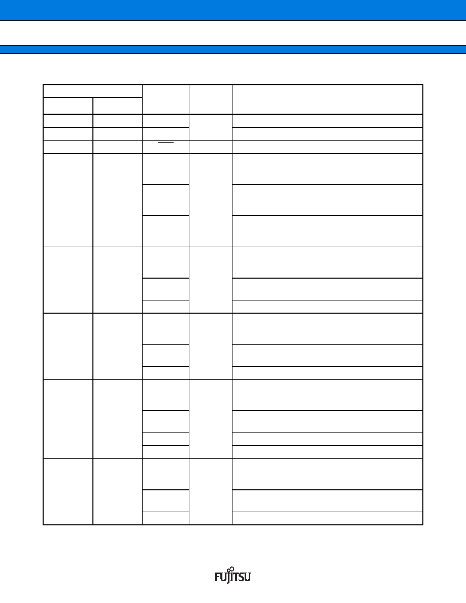
■ PIN DESCRIPTION
(Continued)
Pin No.
Pin name
I/O
Circuit
type*3
Function
LQFP100*1
QFP100*2
90
92
X1
A
Oscillation output pin
91
93
X0
Oscillation input pin
52
54
RST
E
Reset input
75 to 82
77 to 84
P00 to P07
G
General purpose I/O port
The register can be set to select whether to use a pull-
up resistor. This function is enabled in single-chip mode.
AD00
to
AD07
I/O pins for 8 lower bits of the external address/data bus.
This function is enabled when the external bus is
enabled.
INT8
to
INT15
External interrupt request input pins for INT8 to INT15.
83
85
P10
G
General purpose I/O port
The register can be set to select whether to use a pull-
up resistor. This function is enabled in single-chip mode.
AD08
I/O pin of the external address/data bus (AD08). This
function is enabled when the external bus is enabled.
TIN1
Event input pin for the reload timer1
84
86
P11
G
General purpose I/O port
The register can be set to select whether to use a pull-
up resistor. This function is enabled in single-chip mode.
AD09
I/O pin of the external address/data bus (AD09). This
function is enabled when the external bus is enabled.
TOT1
Output pin for the reload timer1
85
87
P12
N
General purpose I/O port
The register can be set to select whether to use a pull-
up resistor. This function is enabled in single-chip mode.
AD10
I/O pin of the external address/data bus (AD10). This
function is enabled when the external bus is enabled.
SIN3
Serial data input pin for UART3
INT11R
External interrupt request input pin (Sub) for INT11
86
88
P13
G
General purpose I/O port
The register can be set to select whether to use a pull-
up resistor. This function is enabled in single-chip mode.
AD11
I/O pin of the external address/data bus (AD11). This
function is enabled when the external bus is enabled.
SOT3
Serial data output pin for UART3
相關(guān)PDF資料 |
PDF描述 |
|---|---|
| MB90P553APF | 16-BIT, OTPROM, 16 MHz, MICROCONTROLLER, PQFP100 |
| MB90W224AZF | 16-BIT, UVPROM, 16 MHz, MICROCONTROLLER, CQFP120 |
| MB90W224AZF | 16-BIT, UVPROM, 16 MHz, MICROCONTROLLER, CQFP120 |
| MB91101APF-G-JNE1 | 32-BIT, 50 MHz, RISC MICROCONTROLLER, PQFP100 |
| MB91106PFV-XXX | 32-BIT, MROM, 50 MHz, RISC MICROCONTROLLER, PQFP100 |
相關(guān)代理商/技術(shù)參數(shù) |
參數(shù)描述 |
|---|---|
| MB90F962SPMCR-GE1 | 制造商:FUJITSU 功能描述:IC MCU 16BIT 16LX 48LQFP |
| MB90F962SPMCR-G-JNE1 | 制造商:FUJITSU 功能描述: |
| MB90V340A-102CR | 制造商:FUJITSU 功能描述: |
| MB-910 | 制造商:Circuit Test 功能描述:BREADBOARD WIRING KIT - 350 PCS |
| MB9100100 | 制造商:COM/DUO 功能描述:FAN 4-6WKS |
發(fā)布緊急采購,3分鐘左右您將得到回復(fù)。