- 您現在的位置:買賣IC網 > PDF目錄102744 > MB90F583CAPF 16-BIT, FLASH, 16 MHz, MICROCONTROLLER, PQFP100 PDF資料下載
參數資料
| 型號: | MB90F583CAPF |
| 元件分類: | 微控制器/微處理器 |
| 英文描述: | 16-BIT, FLASH, 16 MHz, MICROCONTROLLER, PQFP100 |
| 封裝: | 14 X 14 MM, 3,35 MM HEIGHT, 0.65 MM PITCH, PLASTIC, QFP-100 |
| 文件頁數: | 93/112頁 |
| 文件大?。?/td> | 2372K |
| 代理商: | MB90F583CAPF |
第1頁第2頁第3頁第4頁第5頁第6頁第7頁第8頁第9頁第10頁第11頁第12頁第13頁第14頁第15頁第16頁第17頁第18頁第19頁第20頁第21頁第22頁第23頁第24頁第25頁第26頁第27頁第28頁第29頁第30頁第31頁第32頁第33頁第34頁第35頁第36頁第37頁第38頁第39頁第40頁第41頁第42頁第43頁第44頁第45頁第46頁第47頁第48頁第49頁第50頁第51頁第52頁第53頁第54頁第55頁第56頁第57頁第58頁第59頁第60頁第61頁第62頁第63頁第64頁第65頁第66頁第67頁第68頁第69頁第70頁第71頁第72頁第73頁第74頁第75頁第76頁第77頁第78頁第79頁第80頁第81頁第82頁第83頁第84頁第85頁第86頁第87頁第88頁第89頁第90頁第91頁第92頁當前第93頁第94頁第95頁第96頁第97頁第98頁第99頁第100頁第101頁第102頁第103頁第104頁第105頁第106頁第107頁第108頁第109頁第110頁第111頁第112頁
MB90580C Series
DS07-13710-6E
81
2.
Recommended Operating Conditions
(VSS
= AVSS = 0.0 V)
WARNING: The recommended operating conditions are required in order to ensure the normal operation of
the semiconductor device. All of the device's electrical characteristics are warranted when the
device is operated within these ranges.
Always use semiconductor devices within their recommended operating condition ranges.
Operation outside these ranges may adversely affect reliability and could result in device failure.
No warranty is made with respect to uses, operating conditions, or combinations not represented
on the data sheet. Users considering application outside the listed conditions are advised to contact
their representatives beforehand.
Parameter
Symbol
Value
Unit
Remarks
Min
Max
Power supply
voltage
VCC
3.0
5.5
V
Normal operation (MB90583C/CA, MB90587C/CA,
MB90V580B)
4.5
5.5
V
Normal operation
(MB90F583C/CA, MB90F584C/CA)
VCC
3.0
5.5
V
Retains status at the time of operation stop
“H” level input
voltage
VIH
0.7 VCC
VCC
+0.3
V
CMOS input pin
VIHS
0.8 VCC
VCC
+0.3
V
CMOS hysteresis input pin
VIHM
VCC
0.3
VCC
+0.3
V
MD pin input
“L” level input
voltage
VIL
VSS
0.3
0.3 VCC
V
CMOS input pin
VILS
VSS
0.3
0.2 VCC
V
CMOS hysteresis input pin
VILM
VSS
0.3
VSS
+0.3
V
MD pin input
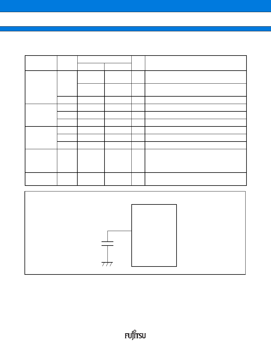
Smoothing
capacitor
CS
0.1
1.0
F
Use a ceramic capacitor or a capacitor with equiv-
alent frequency characteristics. The smoothing ca-
pacitor to be connected to the VCC pin must have a
capacitance value higher than CS.
Operating
temperature
TA
40
+85
°C
C pin connection circuit
C
CS
相關PDF資料 |
PDF描述 |
|---|---|
| M30800SGP-BL | 16-BIT, 20 MHz, MICROCONTROLLER, PQFP100 |
| M30805SGP-BL | 16-BIT, 20 MHz, MICROCONTROLLER, PQFP144 |
| MPC8260ACZUKHBA | 32-BIT, 233 MHz, RISC PROCESSOR, PBGA480 |
| MPC8260CZUHFBC | 32-BIT, 166 MHz, RISC PROCESSOR, PBGA480 |
| MK2069-03GI | 160 MHz, OTHER CLOCK GENERATOR, PDSO56 |
相關代理商/技術參數 |
參數描述 |
|---|---|
| MB90F583CAPFR-GE1 | 制造商:FUJITSU 功能描述: |
| MB90F591GPFR-GE1 | 制造商:FUJITSU 功能描述: |
| MB90F594APFR-GE1 | 制造商:FUJITSU 功能描述: |
| MB90F594GPFR-GE1 | 制造商:FUJITSU 功能描述: |
| MB90F598GPFR-GE1 | 制造商:FUJITSU 功能描述: |
發(fā)布緊急采購,3分鐘左右您將得到回復。