- 您現(xiàn)在的位置:買賣IC網(wǎng) > PDF目錄11741 > MAX9926UAEE/V+ (Maxim Integrated Products)IC VR SENSOR INTERFACE 16QSOP PDF資料下載
參數(shù)資料
| 型號(hào): | MAX9926UAEE/V+ |
| 廠商: | Maxim Integrated Products |
| 文件頁數(shù): | 12/23頁 |
| 文件大?。?/td> | 0K |
| 描述: | IC VR SENSOR INTERFACE 16QSOP |
| 標(biāo)準(zhǔn)包裝: | 100 |
| 系列: | * |
MAX9924–MAX9927
Variable Reluctance Sensor Interfaces with
Differential Input and Adaptive Peak Threshold
2
_______________________________________________________________________________________
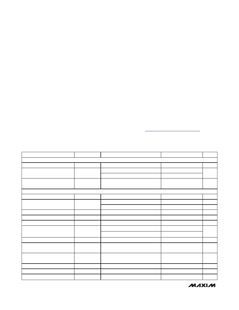
ABSOLUTE MAXIMUM RATINGS
ELECTRICAL CHARACTERISTICS
(VCC = 5V, VGND = 0V, MAX9925/MAX9927 gain setting = 1V/V, Mode A1, VBIAS = 2.5V, VPULLUP = 5V, RPULLUP = 1kΩ, CCOUT =
50pF. TA = TMIN to TMAX, unless otherwise noted. Typical values are at TA = +25°C.) (Note 2)
Stresses beyond those listed under “Absolute Maximum Ratings” may cause permanent damage to the device. These are stress ratings only, and functional
operation of the device at these or any other conditions beyond those indicated in the operational sections of the specifications is not implied. Exposure to
absolute maximum rating conditions for extended periods may affect device reliability.
VCC to GND .............................................................-0.3V to + 6V
All Other Pins..............................................-0.3V to (VCC + 0.3V)
Current into IN+, IN-, IN_+, IN_-.......................................±40mA
Current into All Other Pins ................................................±20mA
Output Short-Circuit (OUT_, OUT) to GND.............................10s
Continuous Power Dissipation (TA = +70°C) (Note 1)
10-Pin MAX (derate 8.8mW/°C above +70°C) ........707.3mW
16-Pin QSOP (derate 9.6mW/°C above +70°C)........771.5mW
Operating Temperature Range .........................-40°C to +125°C
Junction Temperature ......................................................+150°C
Storage Temperature Range .............................-65°C to +150°C
Lead Temperature (soldering, 10s) .................................+300°C
Soldering Temperature (reflow) .......................................+260°C
PARAMETER
SYMBOL
CONDITIONS
MIN
TYP
MAX
UNITS
POWER SUPPLY
Operating Supply Range
VCC
(Note 3)
4.5
5.5
V
MAX9924/MAX9925
2.6
5
Supply Current
ICC
MAX9926/MAX9927
4.7
10
mA
Power-On Time
PON
VCC > VUVLO = 4.1V, step time for VCC
~ 1s
30
150
s
INPUT OPERATIONAL AMPLIFIER (MAX9925/MAX9927)
Input Voltage Range
IN+, IN-
Guaranteed by CMRR
0
VCC
V
Temperature drift
5
V/
°C
Input Offset Voltage
VOS-OA
0.5
3
mV
Input Bias Current
IBIAS
(Note 4)
0.1
6
nA
Input Offset Current
IOFFSET
(Note 4)
0.05
2
nA
Common-Mode Rejection Ratio
CMRR
From VCM = 0 to VCC
75
102
dB
MAX9925
88
105
Power-Supply Rejection Ratio
PSRR
MAX9927
77
94
dB
Output Voltage Low
VOL
IOL = 1mA
0.050
V
Output Voltage High
VOH
IOH = -1mA
VCC -
0.050
V
Recovery Time from Saturation
tSAT
To 1% of the actual VOUT after output
saturates
1.2
s
Gain-Bandwidth Product
GBW
1.4
MHz
Slew Rate
SR
2.3
V/s
Charge-Pump Frequency
fCP
1.3
MHz
Note 1: Package thermal resistances were obtained using the method described in JEDEC specification JESD51-7, using a four-layer
board. For detailed information on package thermal considerations, refer to www.maxim-ic.com/thermal-tutorial.
MAX
Junction-to-Ambient Thermal Resistance (
θJA) ......113.1°C/W
Junction-to-Case Thermal Resistance (
θJC) ................42°C/W
QSOP
Junction-to-Ambient Thermal Resistance (
θJA) ......103.7°C/W
Junction-to-Case Thermal Resistance (
θJC) ................37°C/W
PACKAGE THERMAL CHARACTERISTICS (Note 1)
相關(guān)PDF資料 |
PDF描述 |
|---|---|
| VI-B0T-IX-F3 | CONVERTER MOD DC/DC 6.5V 75W |
| V300B24H150BG | CONVERTER MOD DC/DC 24V 150W |
| VI-B0T-IX-F1 | CONVERTER MOD DC/DC 6.5V 75W |
| V300B24H150BF3 | CONVERTER MOD DC/DC 24V 150W |
| V300B24H150BF2 | CONVERTER MOD DC/DC 24V 150W |
相關(guān)代理商/技術(shù)參數(shù) |
參數(shù)描述 |
|---|---|
| MAX9926UEVKIT+ | 功能描述:磁傳感器開發(fā)工具 Variable-Reluctance Sensor Interface RoHS:否 制造商:Maxim Integrated 工具用于評(píng)估: 接口類型: 工作電壓: |
| MAX9926VAEE+ | 制造商:Maxim Integrated Products 功能描述:- Rail/Tube |
| MAX9926VAEE+T | 制造商:Maxim Integrated Products 功能描述:- Tape and Reel |
| MAX9927AEE/V+ | 功能描述:板機(jī)接口霍耳效應(yīng)/磁性傳感器 Variable-Reluctance Sensor Interface RoHS:否 制造商:Honeywell 類型:Bipolar Hall-Effect Digital Position Sensor 工作電源電壓:3 V to 24 V 電源電流:3.5 mA 最大輸出電流:20 mA 工作點(diǎn)最小值/最大值:5 G, 55 G 最小/最大釋放點(diǎn)(Brp):- 55 G, - 5 G 最大工作溫度:+ 150 C 安裝風(fēng)格:SMD/SMT 封裝 / 箱體:SOT-23 |
| MAX9927AEE/V+T | 功能描述:板機(jī)接口霍耳效應(yīng)/磁性傳感器 Variable-Reluctance Sensor Interface RoHS:否 制造商:Honeywell 類型:Bipolar Hall-Effect Digital Position Sensor 工作電源電壓:3 V to 24 V 電源電流:3.5 mA 最大輸出電流:20 mA 工作點(diǎn)最小值/最大值:5 G, 55 G 最小/最大釋放點(diǎn)(Brp):- 55 G, - 5 G 最大工作溫度:+ 150 C 安裝風(fēng)格:SMD/SMT 封裝 / 箱體:SOT-23 |
發(fā)布緊急采購(gòu),3分鐘左右您將得到回復(fù)。