- 您現(xiàn)在的位置:買賣IC網(wǎng) > PDF目錄384714 > MAX9687MJE (MAXIM INTEGRATED PRODUCTS INC) Octal Bus Transceivers With 3-State Outputs 20-LCCC -55 to 125 PDF資料下載
參數(shù)資料
| 型號: | MAX9687MJE |
| 廠商: | MAXIM INTEGRATED PRODUCTS INC |
| 元件分類: | 運動控制電子 |
| 英文描述: | Octal Bus Transceivers With 3-State Outputs 20-LCCC -55 to 125 |
| 中文描述: | DUAL COMPARATOR, 8000 uV OFFSET-MAX, CDIP16 |
| 封裝: | CERDIP-16 |
| 文件頁數(shù): | 4/4頁 |
| 文件大小: | 44K |
| 代理商: | MAX9687MJE |
Maxim cannot assume responsibility for use of any circuitry other than circuitry entirely embodied in a Maxim product. No circuit patent licenses are
implied. Maxim reserves the right to change the circuitry and specifications without notice at any time.
4
___________________Maxim Integrated Produc ts, 120 S an Gabriel Drive, S unnyvale, CA 94086 (408) 737-7600
1993 Maxim Integrated Products
Printed USA
is a registered trademark of Maxim Integrated Products.
M
Dual, Ultra-Fast ECL-Output Comparator
minimum slew-rate requirements. The tendency of the
part to oscillate is a function of the layout and source
impedance of the circuit employed. Both poor layout
and larger source impedance will increase the mini-
mum slew-rate specification.
In many applications, the addition of regenerative feed-
back will assist the input signal through the linear
region, which will lower the minimum slew-rate require-
ment considerably. For example, with the addition of
positive feedback components Rf = 1k
and
Cf = 10pF, the minimum slew-rate requirement can be
reduced by a factor of four.
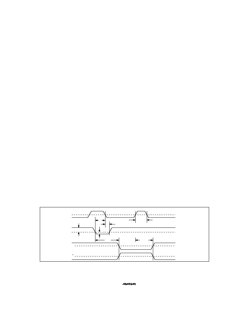
____________________T iming Diagram
The timing diagram (Figure 3) illustrates the series of
events that complete the compare function, under
worst-case conditions.
The top line of the diagram illustrates two latch-enable
(LE) pulses; each pulse is high for the compare func-
tion and low for the latch function. The first pulse
demonstrates the compare function in which part of the
input action takes place during the compare mode.
The second pulse demonstrates a compare-function
interval during which there is no change in the input.
The leading edge of the input signal (illustrated as a
large-amplitude, small-overdrive. Outputs Q and –Q
comparator after time interval t
pd
are similar in timing. The input signal must occur at time
t
s
before the latch falling edge and, to be acquired,
must be maintained for time t
h
after the edge. After t
h
,
the output is no longer affected by the input status until
the latch is again strobed. A minimum latch pulse width
of t
pw
(E) is needed for the strobe operation, and the
output transitions occur after a time t
pd
(E).
Definition of T erms
V
OS
Input Offset Voltage—The voltage required
between the input terminals to obtain 0V differ-
ential at the output.
Input Voltage Pulse Amplitude
Input Voltage Overdrive
Input to Output High Delay—The propagation
delay measured from the time the input signal
crosses the input offset voltage to the 50% point
of an output low-to-high transition.
Input to Output Low Delay—The propagation
delay measured from the time the input signal
crosses the input offset voltage to the 50% point
of an output high-to-low transition.
t
pd+
(E) Latch-Enable to Output High Delay—The propa-
gation delay measured from the 50% point of the
latch-enable signal low-to-high transition to the
50% point of an output low-to-high transition.
t
pd-
(E)
Latch-Enable to Output Low Delay—The propa-
gation delay measured from the 50% point of the
latch-enable signal low-to-high transition to the
50% point of an output high-to-low transition.
t
pw
(E)
Minimum Latch-Enable Pulse Width—The mini-
mum time the latch-enable signal must be high
to acquire and hold an input signal.
t
s
Minimum Setup Time—The minimum time before
the negative transition of the latch-enable pulse
that an input signal must be present to be
acquired and held at the outputs.
t
h
Minimum Hold Time—The minimum time after
the negative transition of the latch-enable signal
that an input signal must remain unchanged to
be acquired and held at the outputs.
V
IN
V
OD
t
pd+
t
pd-
Figure 3. Timing Diagram
LATCH
ENABLE
DIFFERENTIAL
INPUT
VOLTAGE
Q
Q
LATCH
COMPARE
t
s
th
V
OD
V
IN
t
pd
(E)
V
OS
50%
50%
50%
t
pw
(E)
t
pd
相關(guān)PDF資料 |
PDF描述 |
|---|---|
| MAX9687CPE | Dual, Ultra-Fast ECL-Output Comparator |
| MAX9687CJE | Dual, Ultra-Fast ECL-Output Comparator |
| MAX969EEE | Single/Dual/Quad, Micropower, Ultra-Low-Voltage, Rail-to-Rail I/O Comparators |
| MAX965-MAX970 | Single/Dual/Quad, Micropower, Ultra-Low-Voltage, Rail-to-Rail I/O Comparators |
| MAX968 | Single/Dual/Quad, Micropower, Ultra-Low-Voltage, Rail-to-Rail I/O Comparators |
相關(guān)代理商/技術(shù)參數(shù) |
參數(shù)描述 |
|---|---|
| MAX9687MJE-4 | 制造商:Maxim Integrated Products 功能描述:CONTACT FACTORY - Rail/Tube |
| MAX9688ETI+C97 | 制造商:Maxim Integrated Products 功能描述:16-CHANNEL 10-BIT PROGRAMMABLE GAMMA AND VCOM REFERENCE VOLT - Rail/Tube |
| MAX968ESA | 功能描述:校驗器 IC Dual Comparator / Reference RoHS:否 制造商:STMicroelectronics 產(chǎn)品: 比較器類型: 通道數(shù)量: 輸出類型:Push-Pull 電源電壓-最大:5.5 V 電源電壓-最小:1.1 V 補償電壓(最大值):6 mV 電源電流(最大值):1350 nA 響應(yīng)時間: 最大工作溫度:+ 125 C 安裝風(fēng)格:SMD/SMT 封裝 / 箱體:SC-70-5 封裝:Reel |
| MAX968ESA+ | 功能描述:校驗器 IC Dual Comparator / Reference RoHS:否 制造商:STMicroelectronics 產(chǎn)品: 比較器類型: 通道數(shù)量: 輸出類型:Push-Pull 電源電壓-最大:5.5 V 電源電壓-最小:1.1 V 補償電壓(最大值):6 mV 電源電流(最大值):1350 nA 響應(yīng)時間: 最大工作溫度:+ 125 C 安裝風(fēng)格:SMD/SMT 封裝 / 箱體:SC-70-5 封裝:Reel |
| MAX968ESA+T | 功能描述:校驗器 IC Dual Comparator / Reference RoHS:否 制造商:STMicroelectronics 產(chǎn)品: 比較器類型: 通道數(shù)量: 輸出類型:Push-Pull 電源電壓-最大:5.5 V 電源電壓-最小:1.1 V 補償電壓(最大值):6 mV 電源電流(最大值):1350 nA 響應(yīng)時間: 最大工作溫度:+ 125 C 安裝風(fēng)格:SMD/SMT 封裝 / 箱體:SC-70-5 封裝:Reel |
發(fā)布緊急采購,3分鐘左右您將得到回復(fù)。