- 您現(xiàn)在的位置:買賣IC網(wǎng) > PDF目錄385554 > MAX9173ESE (MAXIM INTEGRATED PRODUCTS INC) Quad LVDS Line Receiver with Flow-Through Pinout and “In-Path” Fail-Safe PDF資料下載
參數(shù)資料
| 型號(hào): | MAX9173ESE |
| 廠商: | MAXIM INTEGRATED PRODUCTS INC |
| 元件分類: | 通用總線功能 |
| 英文描述: | Quad LVDS Line Receiver with Flow-Through Pinout and “In-Path” Fail-Safe |
| 中文描述: | QUAD LINE RECEIVER, PDSO16 |
| 封裝: | 0.150 INCH, MS-012AC, SOIC-16 |
| 文件頁(yè)數(shù): | 7/14頁(yè) |
| 文件大小: | 285K |
| 代理商: | MAX9173ESE |
第1頁(yè)第2頁(yè)第3頁(yè)第4頁(yè)第5頁(yè)第6頁(yè)當(dāng)前第7頁(yè)第8頁(yè)第9頁(yè)第10頁(yè)第11頁(yè)第12頁(yè)第13頁(yè)第14頁(yè)

Fail-Safe
The MAX9173 fail-safe drives the receiver output high
when the differential input is:
Open
Undriven and shorted
Undriven and terminated
Without fail-safe, differential noise at the input may
switch the receiver and appear as data to the receiving
system. An open input occurs when a cable and termi-
nation are disconnected. An undriven, terminated input
occurs when a cable is disconnected with the termina-
tion still connected across the receiver inputs or when
the driver of a receiver is in high impedance. An undriv-
en, shorted input can occur due to a shorted cable.
“In-Path” vs. “Parallel” Fail-Safe
The MAX9173 has in-path fail-safe that is compatible
with in-path fail-safe receivers, such as the
DS90LV048A. Refer to the MAX9121/MAX9122 data
sheet for pin-compatible receivers with parallel fail-safe
and lower jitter. Refer to the MAX9130 data sheet for a
single LVDS receiver with parallel fail-safe in an SC70
package.
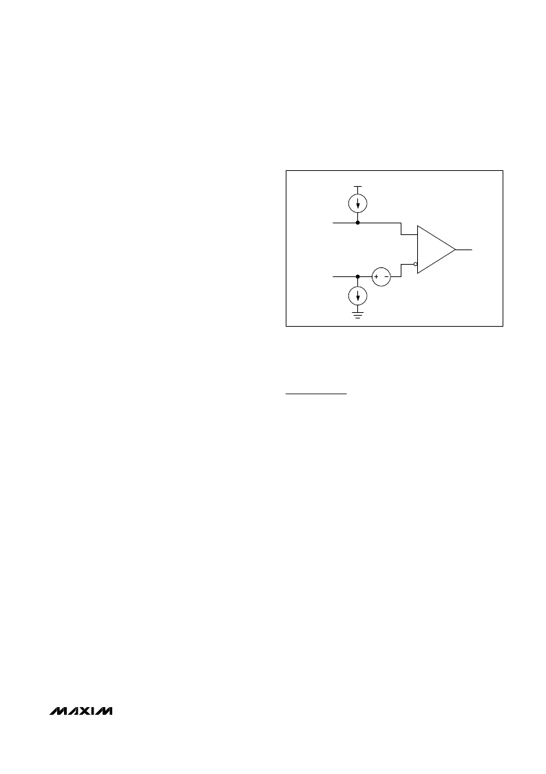
The MAX9173 with in-path fail-safe is designed with a
+45mV input offset voltage, a 2.5μA current source
between V
CC
and the noninverting input, and a 5μA
current sink between the inverting input and ground
(Figure 1). If the differential input is open, the 2.5μA
current source pulls the input to approximately V
CC
-
0.8V and the 5μA current sink pulls the inverting input
to ground, which drives the receiver output high. If the
differential input is shorted or terminated with a typical
value termination resistor, the +45mV offset drives the
receiver output high. If the input is terminated and float-
ing, the receiver output is driven high by the +45mV off-
set, and the 2:1 current sink to current source ratio
(5μA:2.5μA) pulls the inputs to ground. This can be an
advantage when switching between drivers on a multi-
point bus because the change in common-mode volt-
age from ground to the typical driver offset voltage of
1.2V is not as much as the change from V
CC
to 1.2V
(parallel fail-safe pulls the bus to V
CC
).
ESD Protection
ESD-protection structures are incorporated on all pins
to protect against electrostatic discharges encountered
during handling and assembly. The receiver inputs of
the MAX9173 have ±7.0kV of protection against static
electricity (per Human Body Model).
Figure 6a shows the Human Body Model, and Figure
6b shows the current waveform it generates when dis-
charged into a low-impedance load. This model con-
sists of a 100pF capacitor charged to the ESD test volt-
age, which is then discharged into the test device
through a 1.5k
resistor.
Applications Information
Differential Traces
Input trace characteristics affect the performance of the
MAX9173. Use controlled-impedance board traces. For
point-to-point connections, match the receiver input ter-
mination resistor to the differential characteristic imped-
ance of the board traces.
Eliminate reflections and ensure that noise couples as
common mode by running the differential traces close
together. Reduce skew by matching the electrical
length of the traces. Excessive skew can result in a
degradation of magnetic field cancellation.
Each channel
’
s differential signals should be routed
close to each other to cancel their external magnetic
field. Maintain a constant distance between the differ-
ential traces to avoid discontinuities in differential
impedance. Minimize the number of vias to further pre-
vent impedance discontinuities.
Cables and Connectors
LVDS transmission media typically have controlled dif-
ferential impedance of 100
. Use cables and connec-
tors that have matched differential impedance to
minimize impedance discontinuities.
Avoid the use of unbalanced cables such as coaxial
cable. Balanced cables such as twisted pair offer
superior signal quality and tend to generate less EMI
due to magnetic field canceling effects. Balanced
cables pick up noise as common mode, which is reject-
ed by the LVDS receiver.
M
Quad LVDS Line Receiver with Flow-Through
Pinout and “In-Path” Fail-Safe
_______________________________________________________________________________________
7
Figure 1. Input with Fail-Safe Network
V
CC
IN_-
IN_+
OUT_
45mV
5
μ
A
2.5
μ
A
相關(guān)PDF資料 |
PDF描述 |
|---|---|
| MAX9173ETE | Quad LVDS Line Receiver with Flow-Through Pinout and “In-Path” Fail-Safe |
| MAX9173EUE | Quad LVDS Line Receiver with Flow-Through Pinout and “In-Path” Fail-Safe |
| MAX9174ETB | 670MHz LVDS-to-LVDS and Anything-to-LVDS 1:2 Splitters |
| MAX9174EUB | 670MHz LVDS-to-LVDS and Anything-to-LVDS 1:2 Splitters |
| MAX9175ETB | 670MHz LVDS-to-LVDS and Anything-to-LVDS 1:2 Splitters |
相關(guān)代理商/技術(shù)參數(shù) |
參數(shù)描述 |
|---|---|
| MAX9173ESE+ | 制造商:Maxim Integrated Products 功能描述:LINE RCVR 4RX 16SOIC - Rail/Tube |
| MAX9173ESE+T | 制造商:Maxim Integrated Products 功能描述:LINE RCVR 4RX 16SOIC N - Tape and Reel |
| MAX9173ETE | 制造商:Rochester Electronics LLC 功能描述: 制造商:Maxim Integrated Products 功能描述: |
| MAX9173EUE | 制造商:Maxim Integrated Products 功能描述:QUAD LVDS LINE RECEIVER WITH FLOW-THROUGH PIN - Rail/Tube |
| MAX9173EUE+ | 制造商:Maxim Integrated Products 功能描述:LINE RCVR 4RX 16TSSOP - Rail/Tube |
發(fā)布緊急采購(gòu),3分鐘左右您將得到回復(fù)。
