- 您現(xiàn)在的位置:買(mǎi)賣(mài)IC網(wǎng) > PDF目錄383498 > MAX7456 (Maxim Integrated Products, Inc.) Single-Channel Monochrome On-Screen Display with Integrated EEPROM PDF資料下載
參數(shù)資料
第1頁(yè)第2頁(yè)第3頁(yè)第4頁(yè)第5頁(yè)第6頁(yè)第7頁(yè)第8頁(yè)第9頁(yè)當(dāng)前第10頁(yè)第11頁(yè)第12頁(yè)第13頁(yè)第14頁(yè)第15頁(yè)第16頁(yè)第17頁(yè)第18頁(yè)第19頁(yè)第20頁(yè)第21頁(yè)第22頁(yè)第23頁(yè)第24頁(yè)第25頁(yè)第26頁(yè)第27頁(yè)第28頁(yè)第29頁(yè)第30頁(yè)第31頁(yè)第32頁(yè)第33頁(yè)第34頁(yè)第35頁(yè)第36頁(yè)第37頁(yè)第38頁(yè)第39頁(yè)第40頁(yè)第41頁(yè)第42頁(yè)第43頁(yè)
M
Single-Channel Monochrome On-Screen
Display with Integrated EEPROM
10
______________________________________________________________________________________
Detailed Description
The MAX7456 single-channel monochrome on-screen
display (OSD) generator integrates all the functions need-
ed to generate a user-defined OSD and insert it into the
output signal. The MAX7456 accepts a composite NTSC
or PAL video signal. The device includes an input clamp,
sync separator, video timing generator, OSD insertion
mux, nonvolatile character memory, display memory,
OSD generator, crystal oscillator, an SPI-compatible inter-
face to read/write the OSD data, and a video driver (see
the
Simplified Functional Diagram
). Additionally, the
MAX7456 provides vertical sync (
VSYNC
), horizontal
sync (
HSYNC
), and loss-of sync (LOS) outputs for system
synchronization. A clock output signal (CLKOUT) allows
daisy-chaining of multiple devices.
See the
MAX7456 Register Description
section for an
explanation of register notation use in this data sheet.
The 256 user-defined 12 x 18 pixel character set
comes preloaded and is combined with the input video
stream to generate a CVBS signal with OSD video out-
put. A maximum of 256 12 x 18 pixel characters can be
reprogrammed in the NVM. In NTSC mode, 13 rows x
30 characters are displayed. In PAL mode, 16 rows x
30 characters are displayed. When the input video sig-
nal is absent, the OSD image can still be displayed by
using the MAX7456’s internal video timing generator.
Video Input
The MAX7456 accepts standard NTSC or PAL CVBS
signals at VIN. The video signal input must be AC-cou-
pled with a 0.1μF capacitor and is internally clamped.
An input coupling capacitance of 0.1μF is required to
guarantee the specified line-time distortion (LTD) and
video clamp settling time. The video clamp settling time
changes proportionally to the input coupling capaci-
tance, and LTD changes inversely proportional to the
capacitance.
28
27
26
25
24
23
22
21
20
19
18
17
16
15
1
2
3
4
5
6
7
8
9
10
11
12
13
14
MAX7456
N.C.
SDIN
+5V
27MHz
SDOUT
+5V
CVBS OUT
SAG
PGND
RESET
HSYNC
VSYNC
DGND
CLKIN
XFB
CLKOUT
CS
SDIN
SCLK
SDOUT
LOS
N.C.
SCLK
CS
CVBS IN
LOS
VS
HS
N.C.
N.C.
N.C.
CLKOUT
N.C.
AGND
N.C.
N.C.
+5V
0.1
μ
F
C
OUT
75
75
1k
1k
1k
0.1
μ
F
0.1
μ
F
0.1
μ
F
C
SAG
DVDD
VOUT
PVDD
VIN
AVDD
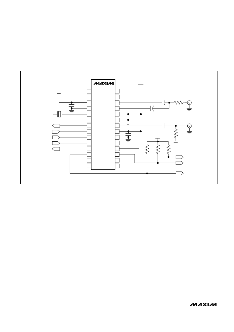
Figure 2. Typical Operating Circuit
相關(guān)PDF資料 |
PDF描述 |
|---|---|
| MAX7462 | Single-Channel Video Reconstruction Filters and Buffers |
| MAX7462USA | Single-Channel Video Reconstruction Filters and Buffers |
| MAX7462UUA | Single-Channel Video Reconstruction Filters and Buffers |
| MAX7463 | Single-Channel Video Reconstruction Filters and Buffers |
| MAX7463USA | Single-Channel Video Reconstruction Filters and Buffers |
相關(guān)代理商/技術(shù)參數(shù) |
參數(shù)描述 |
|---|---|
| MAX7456EUI/GH9 | 制造商:Maxim Integrated Products 功能描述:SINGLE-CHANNEL MONOCHROME ON-SCREEN DISPLAY - Rail/Tube |
| MAX7456EUI+ | 功能描述:視頻 IC Monochrome On Scrn Display Generator RoHS:否 制造商:Fairchild Semiconductor 工作電源電壓:5 V 電源電流:80 mA 最大工作溫度:+ 85 C 封裝 / 箱體:TSSOP-28 封裝:Reel |
| MAX7456EUI+T | 功能描述:視頻 IC Monochrome On Scrn Display Generator RoHS:否 制造商:Fairchild Semiconductor 工作電源電壓:5 V 電源電流:80 mA 最大工作溫度:+ 85 C 封裝 / 箱體:TSSOP-28 封裝:Reel |
| MAX7456EUI+W | 制造商:Maxim Integrated Products 功能描述:- Rail/Tube |
| MAX7456EVKIT | 功能描述:顯示開(kāi)發(fā)工具 RoHS:否 制造商:4D Systems 產(chǎn)品:4Display Shields 工具用于評(píng)估:?OLED-160-G1, ?OLED-160-G2 接口類(lèi)型:Serial 工作電源電壓:5 V |
發(fā)布緊急采購(gòu),3分鐘左右您將得到回復(fù)。