- 您現(xiàn)在的位置:買賣IC網(wǎng) > PDF目錄383481 > MAX6765_0709 (Maxim Integrated Products, Inc.) Automotive Micropower Linear Regulators with Supervisor PDF資料下載
參數(shù)資料
| 型號: | MAX6765_0709 |
| 廠商: | Maxim Integrated Products, Inc. |
| 英文描述: | Automotive Micropower Linear Regulators with Supervisor |
| 中文描述: | 汽車微功耗線性穩(wěn)壓器的監(jiān) |
| 文件頁數(shù): | 17/23頁 |
| 文件大?。?/td> | 309K |
| 代理商: | MAX6765_0709 |
M
Automotive Micropower Linear Regulators
with Supervisor
______________________________________________________________________________________
17
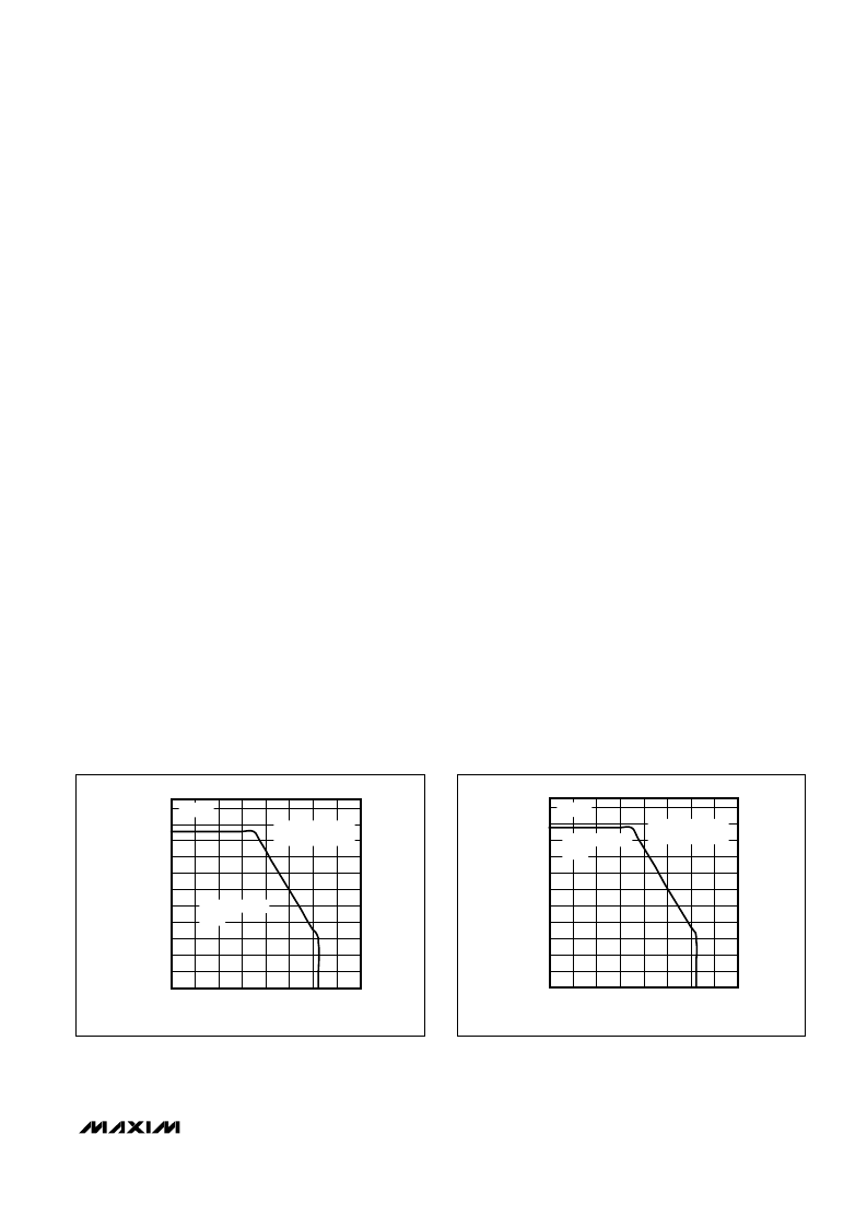
Available Output-Current Calculation
The MAX6765–MAX6774B provide up to 100mA of load
current. Package power dissipation limits the amount of
output current available for a given input/output voltage
and ambient temperature. Figures 3 and 4 depict the
maximum power dissipation curve for the MAX6765/
MAX6766 and MAX6767–MAX6774B, respectively. The
graph assumes that the exposed metal pad of the
device package is soldered to a solid 1in
2
section of
2oz. PCB copper (JESD51-3 AND JESD51-5). Use
Figure 4 to determine the allowable package dissipa-
tion for a given ambient temperature. Alternately, use
the following formula to calculate the allowable pack-
age dissipation:
PD
MAX
= Max. Power Dissip = 1.951W, for T
A
≤
+70°C
PD
MAX
= Max. Power Dissip = [1.9W - 0.0244W x
(T
A
- 70°C)], for +70°C < T
A
≤
+125°C
where 0.0244W is the MAX6767–MAX6774B package
thermal derating in W/°C and T
A
is the ambient tempera-
ture in °C, under the same conditions used for Figure 4.
After determining the allowable package dissipation,
calculate the maximum output current using the follow-
ing formula:
PD < PD
MAX
where PD = [(V
IN
- V
OUT
) x I
OUT
]
Also, I
OUT
should be
≤
100mA in any case.
Selecting Timeout Capacitor
The reset timeout period is adjustable to accommodate
a variety of μP applications. Adjust the reset timeout
period by connecting a capacitor between TIMEOUT
and GND.
t
RP
= C
TIMEOUT
x 1.22 x 10
6
where t
RP
is in seconds and C
TIMEOUT
is in Farads.
Connect TIMEOUT to OUT to select the internally fixed
timeout period. C
TIMEOUT
must be a low-leakage
(< 10nA) type capacitor. Ceramic capacitors are
recommended; do not use capacitor values lower than
100pF to avoid the influence of parasitic capacitances.
Capacitor Selection and
Regulator Stability
For stable operation over the full temperature range and
with load currents up to 100mA, use a 10μF (min) output
capacitor with an ESR < 0.5
. To reduce noise and
improve load-transient response, stability, and power-
supply rejection, use larger output-capacitor values.
Some ceramic dielectrics exhibit large capacitance
and ESR variation with temperature. For dielectric
capacitors such as Z5U and Y5V, use more capaci-
tance to ensure stability at low temperatures. With X7R
or X5R dielectrics, 10μF should be sufficient at all oper-
ating temperatures. For higher-ESR tantalum capaci-
tors, use larger capacitor values to maintain stability. To
improve power-supply rejection and transient
response, use a larger capacitor than the minimum
0.1μF capacitor between IN and GND.
M
TEMPERATURE (
°
C)
P
D
140
120
80
100
40
60
20
0.2
0.4
0.6
0.8
1.0
1.2
1.4
1.6
1.8
2.0
2.2
0
0
160
DERATE 23.8mW/
°
C
ABOVE +70
°
C
1.904W
SAFE OPERATING
AREA
M
TEMPERATURE (
°
C)
P
D
140
120
80
100
40
60
20
0.2
0.4
0.6
0.8
1.0
1.2
1.4
1.6
1.8
2.0
2.2
0
0
160
DERATE 24.4mW/
°
C
ABOVE +70
°
C
1.951W
SAFE OPERATING
AREA
Figure 3. Maximum Power Dissipation vs. Temperature
(MAX6765/MAX6766)
Figure 4. Maximum Power Dissipation vs. Temperature
(MAX6767–MAX6774B)
相關(guān)PDF資料 |
PDF描述 |
|---|---|
| MAX6773B | Automotive Micropower Linear Regulators with Supervisor |
| MAX6774B | Automotive Micropower Linear Regulators with Supervisor |
| MAX6766 | Automotive Micropower Linear Regulators with Supervisor |
| MAX6767 | Automotive Micropower Linear Regulators with Supervisor |
| MAX6768 | Automotive Micropower Linear Regulators with Supervisor |
相關(guān)代理商/技術(shù)參數(shù) |
參數(shù)描述 |
|---|---|
| MAX6765EVKIT+ | 功能描述:電源管理IC開發(fā)工具 MAX6765 Eval Kit RoHS:否 制造商:Maxim Integrated 產(chǎn)品:Evaluation Kits 類型:Battery Management 工具用于評估:MAX17710GB 輸入電壓: 輸出電壓:1.8 V |
| MAX6765TTLD0+ | 制造商:Maxim Integrated Products 功能描述:REG STD LIN ADJ/FIX POS 1.8V TO 11V/5V 0.1A 6TDFN EP - Rail/Tube |
| MAX6765TTLD0+T | 功能描述:線性穩(wěn)壓器 - 標準 uPower Linear Regulator RoHS:否 制造商:STMicroelectronics 輸出類型: 極性: 輸出電壓:1.8 V 輸出電流:150 mA 負載調(diào)節(jié): 最大輸入電壓:5.5 V 線路調(diào)整率: 最大工作溫度:+ 125 C 安裝風(fēng)格:SMD/SMT 封裝 / 箱體:SOT-323-5L |
| MAX6765TTLD1+ | 制造商:Maxim Integrated Products 功能描述:REG STD LIN ADJ/FIX POS 1.8V TO 11V/5V 0.1A 6TDFN EP - Rail/Tube |
| MAX6765TTLD1+T | 功能描述:線性穩(wěn)壓器 - 標準 uPower Linear Regulator RoHS:否 制造商:STMicroelectronics 輸出類型: 極性: 輸出電壓:1.8 V 輸出電流:150 mA 負載調(diào)節(jié): 最大輸入電壓:5.5 V 線路調(diào)整率: 最大工作溫度:+ 125 C 安裝風(fēng)格:SMD/SMT 封裝 / 箱體:SOT-323-5L |
發(fā)布緊急采購,3分鐘左右您將得到回復(fù)。