- 您現(xiàn)在的位置:買賣IC網(wǎng) > PDF目錄224188 > MAX6324AUT46-T (MAXIM INTEGRATED PRODUCTS INC) Analog IC PDF資料下載
參數(shù)資料
| 型號(hào): | MAX6324AUT46-T |
| 廠商: | MAXIM INTEGRATED PRODUCTS INC |
| 元件分類: | 電源管理 |
| 英文描述: | Analog IC |
| 中文描述: | 1-CHANNEL POWER SUPPLY MANAGEMENT CKT, PDSO6 |
| 封裝: | ROHS COMPLIANT, SOT-23, 6 PIN |
| 文件頁數(shù): | 6/13頁 |
| 文件大小: | 168K |
| 代理商: | MAX6324AUT46-T |
MAX6323/MAX6324
P Supervisory Circuits with Windowed
(Min/Max) Watchdog and Manual Reset
2
_______________________________________________________________________________________
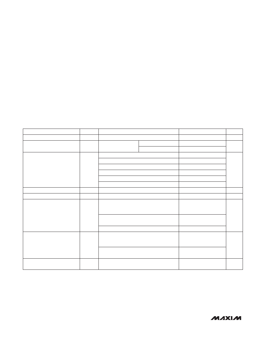
ABSOLUTE MAXIMUM RATINGS
ELECTRICAL CHARACTERISTICS
(VCC = full range, TA = -40°C to +125°C, unless otherwise noted. Typical values are at VCC = 3V, TA = +25°C.) (Note 1)
Stresses beyond those listed under “Absolute Maximum Ratings” may cause permanent damage to the device. These are stress ratings only, and functional
operation of the device at these or any other conditions beyond those indicated in the operational sections of the specifications is not implied. Exposure to
absolute maximum rating conditions for extended periods may affect device reliability.
Terminal Voltage (with respect to GND)
VCC ..................................................................-0.3V to +6.0V
MR, RESET (MAX6323), WDI................-0.3V to (VCC + 0.3V)
WDPO, RESET (MAX6324) ..............................-0.3V to +6.0V
Input Current, VCC, WDI, MR ..............................................20mA
Output Current, RESET, WDPO ..........................................20mA
Rate of Rise, VCC ............................................................100V/s
Continuous Power Dissipation (TA = +70°C)
6-Pin SOT23 (derate 8.7mW/°C above +70°C) ..........696mW
Operating Temperature Range .........................-40°C to +125°C
Junction Temperature ......................................................+150°C
Storage Temperature Range .............................-65°C to +150°C
Lead Temperature (soldering, 10s) .................................+300°C
Soldering Temperature (reflow)
Lead(Pb)-Free ............................................................+260°C
Containing Lead.........................................................+240°C
PARAMETER
SYMBOL
MIN
TYP
MAX
UNITS
4.25
4.38
4.50
4.63
4.75
Supply Current
ICC
27
57
A
Operating Voltage Range
1.2
5.5
VCC
V
VCC = 5.5V
VCC = 2.5V or 3.3V
23
45
A
1
V RESET = V WDPO = +5.5V, RESET, WDPO
deasserted
ILKG
WDPO, RESET Output Leakage
V
VCC - 1.5
ISOURCE = 800A, VCC = 4.75V, RESET
deasserted, (MAX632_ _UT44, MAX632_ _UT46)
VOH
RESET Output Voltage
(MAX6323)
0.8 x VCC
ISOURCE = 500A, VCC = 3.15V, RESET
deasserted (MAX632_ _UT23, MAX632_ _UT26,
MAX632_ _UT29, MAX632_ _UT31)
V
0.4
ISINK = 100A, VCC > 1.2V, RESET asserted
VOL
WDPO, RESET Output Voltage
0.4
ISINK = 3.2mA, VCC = 4.25V (MAX632_ _UT44,
MAX632_ _UT46)
0.4
ISINK = 1.2mA, VCC = 2.25V (MAX632_ _UT23,
MAX632_ _UT26, MAX632_ _UT29,
MAX632_ _UT31)
s
20
10mV/ms, VTH +100mV to VTH - 100mV
VCC to RESET Delay
ms
100
180
280
RESET deasserted
tRP
Reset Timeout Delay
V
2.25
2.32
2.38
CONDITIONS
MAX632_ _UT23
VTH
Reset Threshold Voltage
MAX632_ _UT44
MAX632_ _UT46
No load, RESET
deasserted
2.55
2.63
2.70
MAX632_ _UT26
2.85
2.93
3.00
MAX632_ _UT29
3.00
3.08
3.15
MAX632_ _UT31
相關(guān)PDF資料 |
PDF描述 |
|---|---|
| MAX6324BUT23-T | Analog IC |
| MAX6324BUT26-T | Analog IC |
| MAX6324FUT44-T | Analog IC |
| MAX6324FUT46-T | Analog IC |
| MAX6324GUT23-T | Analog IC |
相關(guān)代理商/技術(shù)參數(shù) |
參數(shù)描述 |
|---|---|
| MAX6324BUT23 | 制造商:Maxim Integrated Products 功能描述:UP SUPERVISORY CIRCUIT WITH WINDOWE - Cut Tape Product |
| MAX6324BUT23+ | 制造商:Maxim Integrated Products 功能描述:PROCESSOR SUPERVISOR 2.32V 27UA 6PIN SOT-23 - Cut Tape Product |
| MAX6324BUT23+T | 功能描述:監(jiān)控電路 uPower Supervisor RoHS:否 制造商:STMicroelectronics 監(jiān)測電壓數(shù): 監(jiān)測電壓: 欠電壓閾值: 過電壓閾值: 輸出類型:Active Low, Open Drain 人工復(fù)位:Resettable 監(jiān)視器:No Watchdog 電池備用開關(guān):No Backup 上電復(fù)位延遲(典型值):10 s 電源電壓-最大:5.5 V 最大工作溫度:+ 85 C 安裝風(fēng)格:SMD/SMT 封裝 / 箱體:UDFN-6 封裝:Reel |
| MAX6324BUT23-T | 功能描述:監(jiān)控電路 RoHS:否 制造商:STMicroelectronics 監(jiān)測電壓數(shù): 監(jiān)測電壓: 欠電壓閾值: 過電壓閾值: 輸出類型:Active Low, Open Drain 人工復(fù)位:Resettable 監(jiān)視器:No Watchdog 電池備用開關(guān):No Backup 上電復(fù)位延遲(典型值):10 s 電源電壓-最大:5.5 V 最大工作溫度:+ 85 C 安裝風(fēng)格:SMD/SMT 封裝 / 箱體:UDFN-6 封裝:Reel |
| MAX6324BUT26 | 制造商:Maxim Integrated Products 功能描述:UP SUPERVISORY CIRCUIT WITH WINDOWE - Cut Tape Product |
發(fā)布緊急采購,3分鐘左右您將得到回復(fù)。