- 您現(xiàn)在的位置:買賣IC網(wǎng) > PDF目錄383445 > MAX600CPA2 (Maxim Integrated Products, Inc.) AC-to-DC Voltage Converter PDF資料下載
參數(shù)資料
| 型號(hào): | MAX600CPA2 |
| 廠商: | Maxim Integrated Products, Inc. |
| 英文描述: | AC-to-DC Voltage Converter |
| 中文描述: | 交流到直流電壓轉(zhuǎn)換器 |
| 文件頁(yè)數(shù): | 10/12頁(yè) |
| 文件大小: | 195K |
| 代理商: | MAX600CPA2 |
M
Low-Cost, Low-Power, Low-Dropout,
S OT 23-3 Voltage Referenc es
10
______________________________________________________________________________________
Detailed Desc ription
The MAX6001–MAX6005 bandgap references offer a
temperature coefficient of <100ppm/°C and initial accura-
cy of better than 1%. These devices can sink and source
up to 400μA with <200mV of dropout voltage, making
them attractive for use in low-voltage applications.
Applic ations Information
Output/Load Capac itanc e
Devices in this family do not require an output capaci-
tance for frequency stability. They are stable for capac-
itive loads from 0 to 2.2nF. However, in applications
where the load or the supply can experience step
changes, an output capacitor will reduce the amount of
overshoot (or undershoot) and assist the circuit’s tran-
sient response. Many applications do not need an
external capacitor, and this family can offer a signifi-
cant advantage in these applications when board
space is critical.
S upply Current
The quiescent supply current of these series-mode ref-
erences is a maximum of 45μA and is virtually indepen-
dent of the supply voltage, with only a 0.8μA/V variation
with supply voltage. Unlike shunt-mode references, the
load current of these series-mode references is drawn
from the supply voltage only when required, so supply
current is not wasted and efficiency is maximized over
the entire supply voltage range. This improved efficien-
cy can help reduce power dissipation and extend bat-
tery life.
When the supply voltage is below the minimum speci-
fied input voltage (as during turn-on), the devices can
draw up to 200μA beyond the nominal supply current.
The input voltage source must be capable of providing
this current to ensure reliable turn-on.
Output V oltage Hysteresis
Output voltage hysteresis is the change in the output
voltage at T
A
= +25°C before and after the device is
cycled over its entire operating temperature range.
Hysteresis is caused by differential package stress
appearing across the bandgap core transistors. The
typical temperature hysteresis value is 130ppm.
Pin Desc ription
NAME
IN
OUT
GND
FUNCTION
1
2
3
Supply Voltage Input
Reference Voltage Output
Ground
PIN
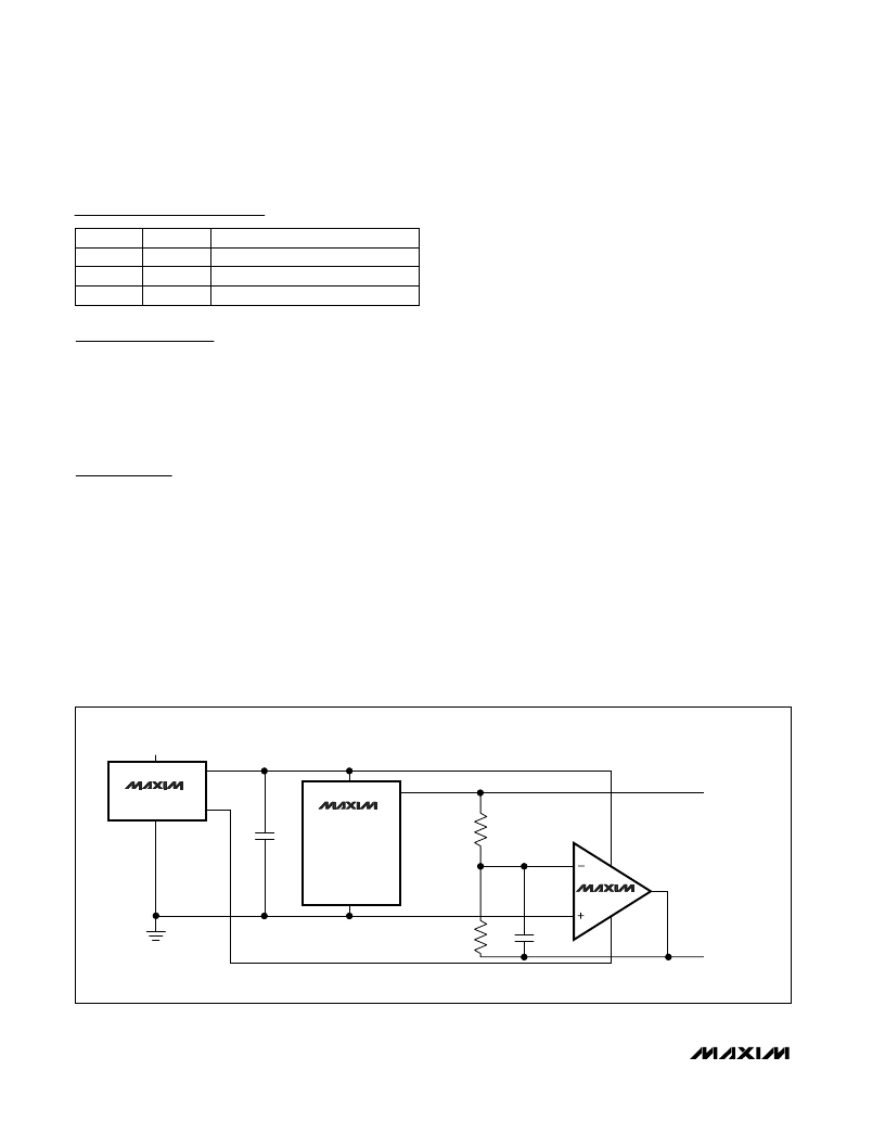
Figure 1. Positive and Negative References from Single +3V or +5V Supply
IN
V
S
+2V
S
-2V
S
OUT
+REF OUTPUT
OUTPUT
-REF OUTPUT
10nF
1M, 0.1%
1M, 0.1%
GND
MAX6001
MAX6002
MAX6003
MAX6004
MAX6005
V
CC
V+
GND
MAX681
V-
V+
V-
ICL7652
相關(guān)PDF資料 |
PDF描述 |
|---|---|
| MAX600LPA | AC-to-DC Voltage Converter |
| MAX600LPA-2 | AC-to-DC Voltage Converter |
| MAX601CPA2 | AC-to-DC Voltage Converter |
| MAX601LPA-2 | AC-to-DC Voltage Converter |
| MAX6021 | +5V.Serial-Input.Voltage-Output 16-Bit DACs[MAX541/MAX542/MAX541/MAX542/MAX541/MAX542/MAX541ACPA/MAX541ACSA/MAX541ACSA-T/MAX541AEPA/MAX541AESA/MAX541AESA-T/MAX541BC/D/MAX541BCPA/MAX541BCSA/MAX541BCSA-T/MAX541BEPA/MAX541BESA/MAX541BESA-T/MAX541CCPA/MAX541C |
相關(guān)代理商/技術(shù)參數(shù) |
參數(shù)描述 |
|---|---|
| MAX600LPA | 制造商:MAXIM 制造商全稱:Maxim Integrated Products 功能描述:AC-to-DC Voltage Converter |
| MAX600LPA2 | 制造商:MAXIM 制造商全稱:Maxim Integrated Products 功能描述:AC To DC Regulator |
| MAX600LPA-2 | 制造商:MAXIM 制造商全稱:Maxim Integrated Products 功能描述:AC-to-DC Voltage Converter |
| MAX601 | 制造商:MAXIM 制造商全稱:Maxim Integrated Products 功能描述:AC To DC Regulator |
| MAX6010 | 制造商:MAXIM 制造商全稱:Maxim Integrated Products 功能描述:Precision, Micropower, 3V Series Voltage Reference in SOT23 |
發(fā)布緊急采購(gòu),3分鐘左右您將得到回復(fù)。