- 您現(xiàn)在的位置:買(mǎi)賣(mài)IC網(wǎng) > PDF目錄383445 > MAX5946LETX (MAXIM INTEGRATED PRODUCTS INC) Dual PCI Express, Hot-Plug Controller PDF資料下載
參數(shù)資料
| 型號(hào): | MAX5946LETX |
| 廠商: | MAXIM INTEGRATED PRODUCTS INC |
| 元件分類(lèi): | 電源管理 |
| 英文描述: | Dual PCI Express, Hot-Plug Controller |
| 中文描述: | 2-CHANNEL POWER SUPPLY SUPPORT CKT, QCC36 |
| 封裝: | 6 X 6 MM, 0.90 MM HEIGHT, MO-220, QFN-36 |
| 文件頁(yè)數(shù): | 13/23頁(yè) |
| 文件大小: | 1019K |
| 代理商: | MAX5946LETX |
第1頁(yè)第2頁(yè)第3頁(yè)第4頁(yè)第5頁(yè)第6頁(yè)第7頁(yè)第8頁(yè)第9頁(yè)第10頁(yè)第11頁(yè)第12頁(yè)當(dāng)前第13頁(yè)第14頁(yè)第15頁(yè)第16頁(yè)第17頁(yè)第18頁(yè)第19頁(yè)第20頁(yè)第21頁(yè)第22頁(yè)第23頁(yè)
Detailed Description
The MAX5946 dual hot-plug controller is designed for
PCI express applications. The device provides hot-plug
control for 12V, 3.3V, and 3.3V auxiliary supplies of two
PCI express slots. The MAX5946’s logic inputs/outputs
allow interfacing directly with the system hot-plug-man-
agement controller or through an SMBus with an exter-
nal I/O expander. An integrated debounced attention
switch and present-detect signals are included to sim-
plify system design.
The MAX5946 drives four external n-channel MOSFETs
to control the 12V and 3.3V main outputs. The 3.3V aux-
iliary outputs are controlled through internal 0.24
n-
channel MOSFETs. Internal charge pumps provide a
gate drive for the 12V outputs while the gate drive of
the 3.3V output is driven by the 12V input supply. The
3.3V auxiliary outputs are completely independent from
the main outputs with their own charge pumps.
At power-up, the MAX5946 keeps all of the external
MOSFETs off until all supplies rise above their respec-
tive UVLO thresholds. The device keeps the internal
MOSFETs off only until the 3.3VAUXIN supply rises
above its UVLO threshold. Upon a turn-on command,
the MAX5946 enhances the external and internal
MOSFETs slowly with a constant gate current to limit
the power-supply inrush current. The MAX5946 actively
limits the current of all outputs at all times and shuts
down if an overcurrent condition persists for longer
than a programmable overcurrent timeout. Thermal-
protection circuitry also shuts down all outputs if the die
temperature exceeds +150
°
C. After an overcurrent or
overtemperature fault condition, the MAX5946L latches
off while the MAX5946A automatically restarts after a
restart time delay.
The power requirement for PCI express connectors is
defined by the PCI express card specification and
summarized in Table 1.
M
Dual PCI Express, Hot-Plug
Controller
______________________________________________________________________________________
13
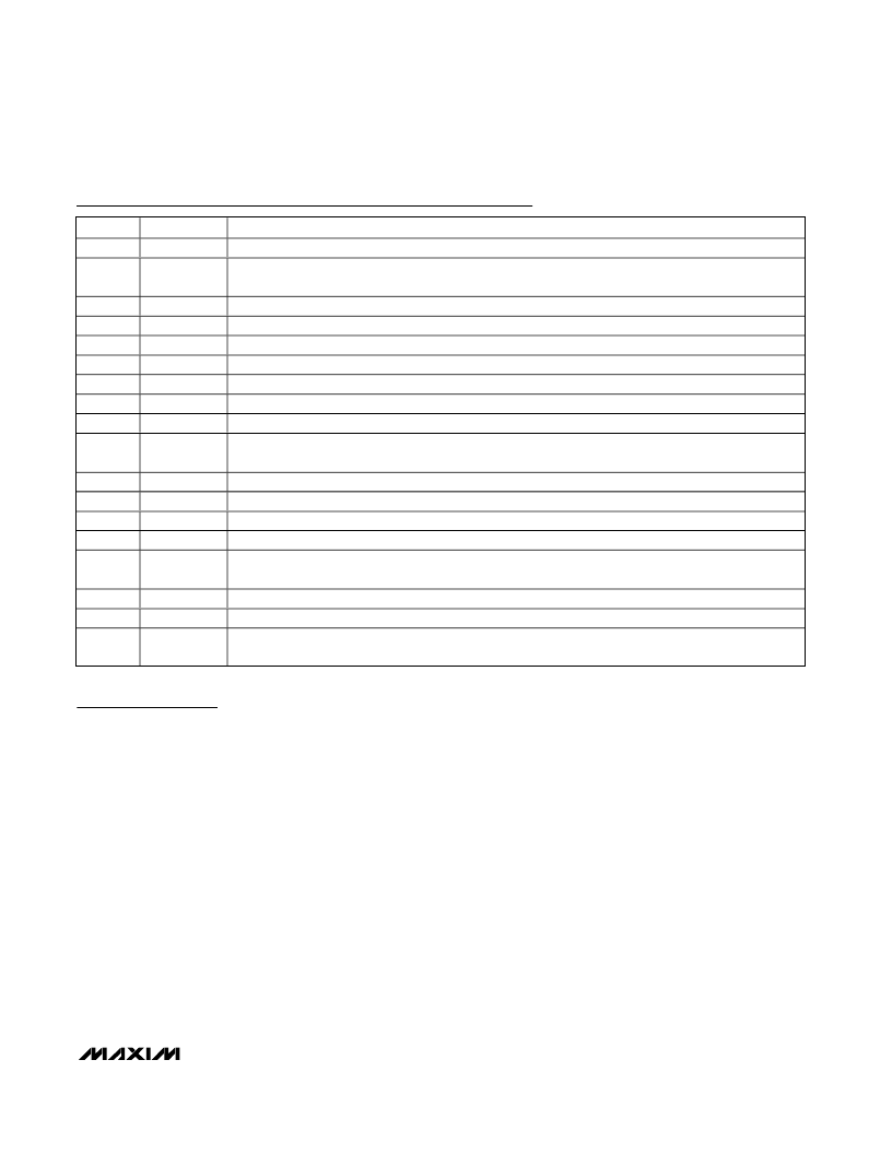
PIN
19
NAME
3.3SB-
FUNCTION
Slot B 3.3V Negative Current-Sense Input. See 3.3SA- function.
20
3.3SB+
Slot B 3.3V Positive Current-Sense Input. Connect the positive side of the current-sense resistor to
3.3SB+ using the Kelvin-sensing technique to assure accurate current sensing.
21
22
23
24
25
26
27
12GB
12SB-
12SB+
AUXONB
ONB
FONB
PRES-DETB
Slot B 12V Gate-Drive Output. See 12GA function.
Slot B 12V Negative Current-Sense Input. See 12SA- function.
Slot B 12V Positive Current-Sense Input. See 12SA+ function.
Slot B 3.3V Auxiliary Output Enable. See AUXONA function.
Slot B 12V And 3.3V Outputs Enable. See ONA function.
Slot B Forced-On Input. See
FONA
function.
Slot B Present-Detect Input. See
PRES-DETA
function.
28
TIM
Overcurrent Timeout Programming Input. Connect a resistor between 500
and 500k
from TIM to GND
to program t
FAULT
. Leave TIM floating for a default timeout of 11ms.
Digital Logic Gate Input
Digital Output. 4ms debounced digital output of INPUT2.
Digital Output. 4ms debounced digital output of INPUT1.
Digital Logic Gate Input
29
30
31
32
INPUT2
OUTPUT2
OUTPUT1
INPUT1
33
12VIN
12V Supply Input. V
12VIN
drives the gates of the MOSFETs connected to 3.3GA and 3.3GB. 12VIN
powers an internal charge pump that drives the gates of the MOSFETs connected to 12GA and 12GB.
34
35
GND
PGND
Ground
Power Ground. Connect externally to GND.
36
PORADJ
Power-On-Reset Programming Input. Connect a resistor between 500
and 500k
from PORADJ to
GND to program the POR timing. Leave floating for a default value of 160ms.
Pin Description (continued)
相關(guān)PDF資料 |
PDF描述 |
|---|---|
| MAX6002EUR | IC-SM-2.5V VOLTAGE REFERENCE |
| MAX6004EUR | IC-SM-4.096V VOLTAGE REFERENCE |
| MAX6023EBK30-T | Analog IC |
| MAX6023EBK41-T | Analog IC |
| MAX6023EBK45-T | Analog IC |
相關(guān)代理商/技術(shù)參數(shù) |
參數(shù)描述 |
|---|---|
| MAX5946LETX+ | 功能描述:熱插拔功率分布 Dual PCIe Hot-Plug Controller RoHS:否 制造商:Texas Instruments 產(chǎn)品:Controllers & Switches 電流限制: 電源電壓-最大:7 V 電源電壓-最小:- 0.3 V 工作溫度范圍: 功率耗散: 安裝風(fēng)格:SMD/SMT 封裝 / 箱體:MSOP-8 封裝:Tube |
| MAX5946LETX+T | 功能描述:熱插拔功率分布 Dual PCIe Hot-Plug Controller RoHS:否 制造商:Texas Instruments 產(chǎn)品:Controllers & Switches 電流限制: 電源電壓-最大:7 V 電源電壓-最小:- 0.3 V 工作溫度范圍: 功率耗散: 安裝風(fēng)格:SMD/SMT 封裝 / 箱體:MSOP-8 封裝:Tube |
| MAX5946LETX-T | 功能描述:熱插拔功率分布 RoHS:否 制造商:Texas Instruments 產(chǎn)品:Controllers & Switches 電流限制: 電源電壓-最大:7 V 電源電壓-最小:- 0.3 V 工作溫度范圍: 功率耗散: 安裝風(fēng)格:SMD/SMT 封裝 / 箱體:MSOP-8 封裝:Tube |
| MAX5946LEVKIT | 功能描述:熱插拔功率分布 RoHS:否 制造商:Texas Instruments 產(chǎn)品:Controllers & Switches 電流限制: 電源電壓-最大:7 V 電源電壓-最小:- 0.3 V 工作溫度范圍: 功率耗散: 安裝風(fēng)格:SMD/SMT 封裝 / 箱體:MSOP-8 封裝:Tube |
| MAX5947AESA | 功能描述:熱插拔功率分布 RoHS:否 制造商:Texas Instruments 產(chǎn)品:Controllers & Switches 電流限制: 電源電壓-最大:7 V 電源電壓-最小:- 0.3 V 工作溫度范圍: 功率耗散: 安裝風(fēng)格:SMD/SMT 封裝 / 箱體:MSOP-8 封裝:Tube |
發(fā)布緊急采購(gòu),3分鐘左右您將得到回復(fù)。