- 您現(xiàn)在的位置:買賣IC網(wǎng) > PDF目錄383442 > MAX5732ACTN (MAXIM INTEGRATED PRODUCTS INC) 32-Channel, 16-Bit, Voltage-Output DACs with Serial Interface PDF資料下載
參數(shù)資料
| 型號(hào): | MAX5732ACTN |
| 廠商: | MAXIM INTEGRATED PRODUCTS INC |
| 元件分類: | DAC |
| 英文描述: | 32-Channel, 16-Bit, Voltage-Output DACs with Serial Interface |
| 中文描述: | SERIAL INPUT LOADING, 20 us SETTLING TIME, 16-BIT DAC, QCC56 |
| 封裝: | 8 X 8 MM, 0.80 MM HEIGHT, MO-220, QFN-56 |
| 文件頁(yè)數(shù): | 2/26頁(yè) |
| 文件大?。?/td> | 451K |
| 代理商: | MAX5732ACTN |
第1頁(yè)當(dāng)前第2頁(yè)第3頁(yè)第4頁(yè)第5頁(yè)第6頁(yè)第7頁(yè)第8頁(yè)第9頁(yè)第10頁(yè)第11頁(yè)第12頁(yè)第13頁(yè)第14頁(yè)第15頁(yè)第16頁(yè)第17頁(yè)第18頁(yè)第19頁(yè)第20頁(yè)第21頁(yè)第22頁(yè)第23頁(yè)第24頁(yè)第25頁(yè)第26頁(yè)

M
32-Channel, 16-Bit, Voltage-Output
DACs with Serial Interface
2
_______________________________________________________________________________________
ABSOLUTE MAXIMUM RATINGS
AV
CC
to V
SS
, AGND, DGND, REFGND..................-0.3V to +12V
V
SS
to AGND, DGND................................................-6V to +0.3V
AV
DD
, DV
DD
to AGND, DGND, REFGND.................-0.3V to +6V
AGND to DGND.....................................................-0.3V to +0.3V
REF to AGND, DGND,
REFGND...............-0.3V to the lower of (AV
DD
+ 0.3V) and +6V
REFGND to AGND.................................................-0.3V to +0.3V
Digital Inputs to AGND, DGND,
REFGND..............-0.3V to the lower of (DVDD+ 0.3V) and +6V
DOUT to DGND.......-0.3V to the lower of (DV
DD
+ 0.3V) and +6V
OUT_ to V
SS
.........-0.3V to the lower of (AV
CC
+ 0.3V) and +12V
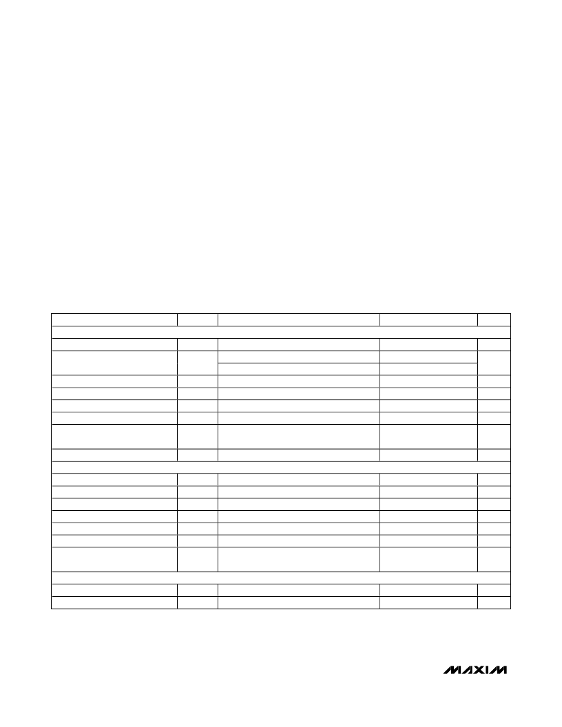
ELECTRICAL CHARACTERISTICS—MAX5732 (0 to +5V Output Voltage Range)
(AV
CC
= +5.25V to +5.5V (Note 1), AV
DD
= +5V ±5%, DV
DD
= +2.7V to AV
DD
, V
SS
= AGND = DGND = REFGND = GS = 0, V
REF
=
+3.0V, R
L
=
∞
, C
L
= 50pF referenced to ground, T
A
= T
MIN
to T
MAX
, unless otherwise noted. Typical values are at T
A
= +25°C.)
Stresses beyond those listed under “Absolute Maximum Ratings” may cause permanent damage to the device. These are stress ratings only, and functional
operation of the device at these or any other conditions beyond those indicated in the operational sections of the specifications is not implied. Exposure to
absolute maximum rating conditions for extended periods may affect device reliability.
GS to AGND................................................................-1V to +1V
Maximum Current into REF...............................................±10mA
Maximum Current into Any Pin.........................................±50mA
Continuous Power Dissipation (T
A
= +70°C)
Thin QFN (derate 31.3mW/°C above +70°C)...................2.5W
Operating Temperature Ranges
MAX573__CTN....................................................0°C to +70°C
MAX573__ETN.................................................-40°C to +85°C
Junction Temperature......................................................+150°C
Storage Temperature Range.............................-65°C to +150°C
Lead Temperature (soldering, 10s).................................+300°C
PARAMETER
SYMBOL
CONDITIONS
MIN
TYP
MAX
UNITS
DC CHARACTERISTICS
Resolution
N
16
Bits
MAX5732B
MAX5732C
Guaranteed monotonic (Note 3)
V
SS
= -0.5V, AV
CC
= +5.25V (Note 4)
(Note 4)
±8
±32
±16
±64
±1
±40
±50
±0.5
Integral Nonlinearity (Note 2)
INL
LSB
Differential Nonlinearity
Zero-Scale Error
Full-Scale Error
Gain Error
DNL
V
OS
LSB
mV
mV
%FSR
±8
±8
±0.1
Gain Temperature Coefficient
20
40
ppm
FSR/°C
DC Crosstalk
DYNAMIC CHARACTERISTICS
Output-Voltage Settling Time
Voltage-Output Slew Rate
Digital Feedthrough
Digital Crosstalk
Digital-to-Analog Glitch Impulse
DAC-to-DAC Crosstalk
V
SS
= -0.5V, AV
CC
= +5V (Note 5)
50
250
μV
Full-scale change to ±0.5 LSB
20
1
5
5
120
15
μs
V/μs
nV-s
nV-s
nV-s
nV-s
(Note 6)
(Note 7)
Major carry transition
(Note 8)
Output Noise Spectral Density at
1kHz
Full-scale code
250
nV/
√
Hz
ANALOG OUTPUTS (OUT0 to OUT31)
Output Voltage Range
Resistive Load to Ground
V
SS
= -0.5V, AV
CC
= +5V
0
10
5
V
50
k
相關(guān)PDF資料 |
PDF描述 |
|---|---|
| MAX5732AETN | 32-Channel, 16-Bit, Voltage-Output DACs with Serial Interface |
| MAX5732BCTN | 32-Channel, 16-Bit, Voltage-Output DACs with Serial Interface |
| MAX5735CCTN | CONNECTOR |
| MAX5735CETN | CONNECTOR |
| MAX5732BETN | 32-Channel, 16-Bit, Voltage-Output DACs with Serial Interface |
相關(guān)代理商/技術(shù)參數(shù) |
參數(shù)描述 |
|---|---|
| MAX5732ACTN-T | 制造商:Maxim Integrated Products 功能描述:16-BIT 32 CHANNEL 0 - 5V VOUT DAC - Tape and Reel |
| MAX5732AETN | 制造商:Maxim Integrated Products 功能描述:16-BIT 32 CHANNEL 0 - 5V VOUT DAC - Rail/Tube |
| MAX5732AETN-T | 制造商:Maxim Integrated Products 功能描述:16-BIT 32 CHANNEL 0 - 5V VOUT DAC - Tape and Reel |
| MAX5732AUCB | 制造商:Maxim Integrated Products 功能描述:16-BIT 32 CHANNEL 0 - 5V VOUT DAC - Rail/Tube |
| MAX5732AUTN | 功能描述:數(shù)模轉(zhuǎn)換器- DAC RoHS:否 制造商:Texas Instruments 轉(zhuǎn)換器數(shù)量:1 DAC 輸出端數(shù)量:1 轉(zhuǎn)換速率:2 MSPs 分辨率:16 bit 接口類型:QSPI, SPI, Serial (3-Wire, Microwire) 穩(wěn)定時(shí)間:1 us 最大工作溫度:+ 85 C 安裝風(fēng)格:SMD/SMT 封裝 / 箱體:SOIC-14 封裝:Tube |
發(fā)布緊急采購(gòu),3分鐘左右您將得到回復(fù)。