- 您現(xiàn)在的位置:買賣IC網(wǎng) > PDF目錄384680 > MAX496CPE (MAXIM INTEGRATED PRODUCTS INC) High-Output RS-485 Transceiver 8-PDIP -40 to 85 PDF資料下載
參數(shù)資料
| 型號(hào): | MAX496CPE |
| 廠商: | MAXIM INTEGRATED PRODUCTS INC |
| 元件分類: | 運(yùn)動(dòng)控制電子 |
| 英文描述: | High-Output RS-485 Transceiver 8-PDIP -40 to 85 |
| 中文描述: | QUAD BUFFER AMPLIFIER, PDIP16 |
| 封裝: | PLASTIC, DIP-16 |
| 文件頁數(shù): | 11/12頁 |
| 文件大小: | 219K |
| 代理商: | MAX496CPE |
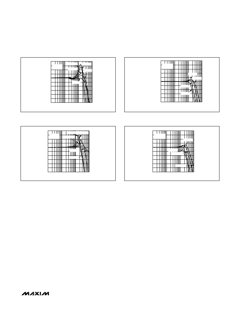
The MAX496/MAX497 drive capacitive loads up to 75pF
without sustained oscillation, although some peaking
may occur. When driving larger capacitive loads, or to
reduce peaking, add an isolation resistor (R
ISO
) between
the output and the capacitive load (Figures 5a–5d).
Grounding and Layout
The MAX496/MAX497 bandwidths are in the RF fre-
quency range. Depending on the size of the PC board
used and the frequency of operation, it may be neces-
sary to use Micro-strip or Stripline techniques.
To realize the full AC performance of these high-speed
buffers, pay careful attention to power-supply bypassing
and board layout. The PC board should have at least two
layers (wire-wrap boards are too inductive, bread boards
are too capacitive), with one side a signal layer and the
other a large, low-impedance ground plane. With multilay-
er boards, locate the ground plane on the layer that is not
dedicated to a specific signal trace. The ground plane
should be as free from voids as possible. Connect all
ground pins to the ground plane.
Connect both positive power-supply pins together and
bypass with a 0.10μF ceramic capacitor at each power
supply pin, as close to the device as possible. Repeat
the same for the negative power-supply pins. The
capacitor lead lengths should be as short as possible
to minimize lead inductance; surface-mount chip
capacitors are ideal. A large-value (4.7μF or greater)
tantalum or electrolytic bypass capacitor on each sup-
ply may be required for high-current loads. The location
of this capacitor is not critical.
The MAX496/MAX497’s analog input pins are isolated
with ground pins to minimize parasitic coupling, which can
degrade crosstalk and/or amplifier stability. Keep signal
paths as short as possible to minimize inductance. Ensure
that all input channel traces are the same length to main-
tain the phase relationship between the four channels. To
further reduce crosstalk, connect the coaxial-cable shield
to the ground side of the 75
terminating resistor at the
ground plane, and terminate all unused inputs ground and
outputs with a 100
or 150
resistor to ground.
M
375MHz Quad Closed-Loop
Video Buffers, A
V
= +1 and +2
______________________________________________________________________________________
11
1M
10M
FREQUENCY (Hz)
1G
-12
-10
-8
-6
-4
-2
0
2
4
6
8
M
G
100M
C
L
= 22pF
C
L
= 10pF
C
L
= 0pF
C
L
= 47pF
C
L
= 60pF
R
L
= 50
R
ISO
= 0
Figure 5a. MAX496 Small-Signal Gain vs. Frequency and Load
Capacitor (R
L
= 50
, R
ISO
= 0
)
1M
10M
FREQUENCY (Hz)
1G
-30
-25
-20
-15
-10
-5
0
5
10
15
20
M
G
100M
C
L
= 10pF
C
L
= 0pF
C
L
= 47pF
C
L
= 68pF
R
L
=
R
ISO
= 0
8
C
L
= 20pF
1M
10M
FREQUENCY (Hz)
1G
-30
-25
-20
-15
-10
-5
0
5
10
15
20
M
G
100M
C
L
= 10pF
C
L
= 47pF
R
L
=
R
ISO
= 20
C
L
= 22pF
C
L
= 68pF
8
Figure 5c. MAX496 Small-Signal Gain vs. Frequency and Load
Capacitor (R
L
=
∞
, R
ISO
= 0
)
1M
10M
FREQUENCY (Hz)
1G
-5
-4
-3
-2
-1
0
1
2
3
4
5
M
* -3dB ATTENUATION DUE
TO R
ISO
NOT SHOWN
G
100M
C
L
= 22pF
C
L
= 10pF
C
L
= 47pF
R
L
= 50
R
ISO
= 20
C
L
= 60pF
Figure 5b. MAX496 Small-Signal Gain vs. Frequency and
Load Capacitor (R
L
= 50
, R
ISO
= 20
)
Figure 5d. MAX496 Small-Signal Gain vs. Frequency and
Load Capacitor (R
L
=
∞
, R
ISO
= 20
)
相關(guān)PDF資料 |
PDF描述 |
|---|---|
| MAX496CSE | High-Output RS-485 Transceiver 8-SOIC -40 to 85 |
| MAX497CPE | High-Output RS-485 Transceiver 8-SOIC -40 to 85 |
| MAX497CSE | High-Output RS-485 Transceiver 8-SOIC -40 to 85 |
| MAX498CWI | Quad/Triple, SPDT, RGB Switches with 250MHz Video Buffer Amplifiers |
| MAX499 | 30 AMP MINIATURE POWER RELAY |
相關(guān)代理商/技術(shù)參數(shù) |
參數(shù)描述 |
|---|---|
| MAX496CPE+ | 功能描述:運(yùn)算放大器 - 運(yùn)放 RoHS:否 制造商:STMicroelectronics 通道數(shù)量:4 共模抑制比(最小值):63 dB 輸入補(bǔ)償電壓:1 mV 輸入偏流(最大值):10 pA 工作電源電壓:2.7 V to 5.5 V 安裝風(fēng)格:SMD/SMT 封裝 / 箱體:QFN-16 轉(zhuǎn)換速度:0.89 V/us 關(guān)閉:No 輸出電流:55 mA 最大工作溫度:+ 125 C 封裝:Reel |
| MAX496CSE | 功能描述:運(yùn)算放大器 - 運(yùn)放 RoHS:否 制造商:STMicroelectronics 通道數(shù)量:4 共模抑制比(最小值):63 dB 輸入補(bǔ)償電壓:1 mV 輸入偏流(最大值):10 pA 工作電源電壓:2.7 V to 5.5 V 安裝風(fēng)格:SMD/SMT 封裝 / 箱體:QFN-16 轉(zhuǎn)換速度:0.89 V/us 關(guān)閉:No 輸出電流:55 mA 最大工作溫度:+ 125 C 封裝:Reel |
| MAX496CSE+ | 功能描述:運(yùn)算放大器 - 運(yùn)放 RoHS:否 制造商:STMicroelectronics 通道數(shù)量:4 共模抑制比(最小值):63 dB 輸入補(bǔ)償電壓:1 mV 輸入偏流(最大值):10 pA 工作電源電壓:2.7 V to 5.5 V 安裝風(fēng)格:SMD/SMT 封裝 / 箱體:QFN-16 轉(zhuǎn)換速度:0.89 V/us 關(guān)閉:No 輸出電流:55 mA 最大工作溫度:+ 125 C 封裝:Reel |
| MAX496CSE+T | 功能描述:運(yùn)算放大器 - 運(yùn)放 RoHS:否 制造商:STMicroelectronics 通道數(shù)量:4 共模抑制比(最小值):63 dB 輸入補(bǔ)償電壓:1 mV 輸入偏流(最大值):10 pA 工作電源電壓:2.7 V to 5.5 V 安裝風(fēng)格:SMD/SMT 封裝 / 箱體:QFN-16 轉(zhuǎn)換速度:0.89 V/us 關(guān)閉:No 輸出電流:55 mA 最大工作溫度:+ 125 C 封裝:Reel |
| MAX496CSE-T | 功能描述:運(yùn)算放大器 - 運(yùn)放 RoHS:否 制造商:STMicroelectronics 通道數(shù)量:4 共模抑制比(最小值):63 dB 輸入補(bǔ)償電壓:1 mV 輸入偏流(最大值):10 pA 工作電源電壓:2.7 V to 5.5 V 安裝風(fēng)格:SMD/SMT 封裝 / 箱體:QFN-16 轉(zhuǎn)換速度:0.89 V/us 關(guān)閉:No 輸出電流:55 mA 最大工作溫度:+ 125 C 封裝:Reel |
發(fā)布緊急采購(gòu),3分鐘左右您將得到回復(fù)。