- 您現(xiàn)在的位置:買賣IC網(wǎng) > PDF目錄383376 > MAX4002EBL-T (MAXIM INTEGRATED PRODUCTS INC) 2.5GHz 45dB RF-Detecting Controllers PDF資料下載
參數(shù)資料
| 型號: | MAX4002EBL-T |
| 廠商: | MAXIM INTEGRATED PRODUCTS INC |
| 元件分類: | 運動控制電子 |
| 英文描述: | 2.5GHz 45dB RF-Detecting Controllers |
| 中文描述: | LOG OR ANTILOG AMPLIFIER, 2400 MHz BAND WIDTH, BGA8 |
| 封裝: | UCSP-8 |
| 文件頁數(shù): | 13/18頁 |
| 文件大小: | 670K |
| 代理商: | MAX4002EBL-T |

M
2.5GHz 45dB RF-Detecting Controllers
______________________________________________________________________________________
13
Detailed Description
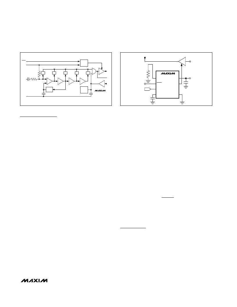
The MAX4000/MAX4001/MAX4002 family of logarithmic
amplifiers (log amps) is comprised of four main amplifi-
er/limiter stages each with a small-signal gain of 10dB.
The output stage of each amplifier is applied to a full-
wave rectifier (detector). A detector stage also pre-
cedes the first gain stage. In total, five detectors each
separated by 10dB, comprise the log amp strip. Figure
1 shows the functional diagram of the log amps.
A portion of the PA output power is coupled to RFIN of
the log amp controller, and is applied to the log amp
strip. Each detector cell outputs a rectified current and
all cell currents are summed and form a logarithmic
output. The detected output is applied to a high-gain
g
m
stage, which is buffered and then applied to OUT.
OUT is applied to the gain-control pin of the PA to close
the control loop. The voltage applied to SET determines
the output power of the PA in the control loop. The volt-
age applied to SET relates to an input power level
determined by the log amp detector characteristics.
Extrapolating a straight-line fit of the graph of SET vs.
RFIN provides the logarithmic intercept. Logarithmic
slope, the amount SET changes for each dB change of
RF input, is generally independent of waveform or ter-
mination impedance. The MAX4000/MAX4001/
MAX4002 slope at low frequencies is about 25mV/dB.
Variance in temperature and supply voltage does not
alter the slope significantly as shown in the
Typical
Operating Characteristics
.
The MAX4000/MAX4001/MAX4002 are specifically des-
igned for use in PA control applications. In a control
loop, the output starts at approximately 2.9V (with sup-
ply voltage of 3V) for the minimum input signal and falls
to a value close to ground at the maximum input. With a
portion of the PA output power coupled to RFIN, apply
a voltage to SET and connect OUT to the gain-control
pin of the PA to control its output power. An external
capacitor from the CLPF pin to ground sets the band-
width of the PA control loop.
Transfer Function
Logarithmic slope and intercept determine the transfer
function of the MAX4000/MAX4001/MAX4002 family of
log amps. The change in SET voltage per dB change in
RF input defines the logarithmic slope. Therefore, a
10dB change in RF input results in a 250mV change at
SET. The Log-Conformance plots (see
Typical Oper-
ating Characteristics
) show the dynamic range of the
log amp family. Dynamic range is the range for which
the error remains within a band of ±1dB.
The intercept is defined as the point where the linear
response, when extrapolated, intersects the y-axis of
the Log-Conformance plot. Using these parameters,
the input power can be calculated at any SET voltage
level within the specified input range with the following
equation:
SET
SLOPE
where SET is the set-point voltage, SLOPE is the loga-
rithmic slope (V/dB), RFIN is in either dBm or dBV and
IP is the logarithmic intercept point utilizing the same
units as RFIN.
Applications Information
Controller Mode
Figure 2 provides a circuit example of the MAX4000/
MAX4001/MAX4002 configured as a controller. The
MAX4000/MAX4001/MAX4002 require a 2.7V to 5.5V
supply voltage. Place a 0.1μF low-ESR, surface-mount
ceramic capacitor close to V
CC
to decouple the supply.
Electrically isolate the RF input from other pins (espe-
cially SET) to maximize performance at high frequencies
(especially at the high-power levels of the MAX4002).
The MAX4000 has an internal input-coupling capacitor
RFIN
IP
=
+
Figure 1. Functional Diagram
V
CC
OUT
N.C.
GND
CLPF
SET
RFIN
MAX4000
SHDN
DAC
RF INPUT
V
CC
V
CC
XX
POWER AMPLIFIER
ANTENNA
50
C
F
0.1
μ
F
Figure 2. Controller Mode Application Circuit Block
10dB
DET
10dB
10dB
10dB
DET
DET
DET
DET
OFFSET
COMP
LOW-
BNOISE
OUTPUT
DELAY
GND
(PADDLE)
gm
+
-
X1
V-I
RFIN
V
CC
SHDN
OUT
CLPF
SET
MAX4000
相關(guān)PDF資料 |
PDF描述 |
|---|---|
| MAX4000 | 2.5GHz 45dB RF-Detecting Controllers |
| MAX4001 | 2.5GHz 45dB RF-Detecting Controllers |
| MAX4002 | 2.5GHz 45dB RF-Detecting Controllers |
| MAX4002EUA | 2.5GHz 45dB RF-Detecting Controllers |
| MAX4003ETA-T | 100MHz to 2500MHz, 45dB RF Detector in a UCSP |
相關(guān)代理商/技術(shù)參數(shù) |
參數(shù)描述 |
|---|---|
| MAX4002EUA | 功能描述:射頻檢測器 2.5GHz 45dB RF Detecting Ctlr RoHS:否 制造商:Skyworks Solutions, Inc. 配置: 頻率范圍:650 MHz to 3 GHz 最大二極管電容: 最大工作溫度:+ 85 C 最小工作溫度:- 40 C 封裝 / 箱體:SC-88 封裝:Reel |
| MAX4002EUA+ | 功能描述:射頻檢測器 2.5GHz 45dB RF Detecting Ctlr RoHS:否 制造商:Skyworks Solutions, Inc. 配置: 頻率范圍:650 MHz to 3 GHz 最大二極管電容: 最大工作溫度:+ 85 C 最小工作溫度:- 40 C 封裝 / 箱體:SC-88 封裝:Reel |
| MAX4002EUA+T | 功能描述:射頻檢測器 2.5GHz 45dB RF Detecting Ctlr RoHS:否 制造商:Skyworks Solutions, Inc. 配置: 頻率范圍:650 MHz to 3 GHz 最大二極管電容: 最大工作溫度:+ 85 C 最小工作溫度:- 40 C 封裝 / 箱體:SC-88 封裝:Reel |
| MAX4002EUA-T | 功能描述:射頻檢測器 2.5GHz 45dB RF Detecting Ctlr RoHS:否 制造商:Skyworks Solutions, Inc. 配置: 頻率范圍:650 MHz to 3 GHz 最大二極管電容: 最大工作溫度:+ 85 C 最小工作溫度:- 40 C 封裝 / 箱體:SC-88 封裝:Reel |
| MAX4003 | 制造商:MAXIM 制造商全稱:Maxim Integrated Products 功能描述:100MHz to 2500MHz, 45dB RF Detector in a UCSP |
發(fā)布緊急采購,3分鐘左右您將得到回復。