- 您現(xiàn)在的位置:買賣IC網(wǎng) > PDF目錄384666 > MAX3841ETG (MAXIM INTEGRATED PRODUCTS INC) Dual LVDS Transmitter/Receiver 16-TSSOP -40 to 85 PDF資料下載
參數(shù)資料
| 型號(hào): | MAX3841ETG |
| 廠商: | MAXIM INTEGRATED PRODUCTS INC |
| 元件分類: | 運(yùn)動(dòng)控制電子 |
| 英文描述: | Dual LVDS Transmitter/Receiver 16-TSSOP -40 to 85 |
| 中文描述: | 2-CHANNEL, CROSS POINT SWITCH, QCC24 |
| 封裝: | 4 X 4 MM, TQFN-24 |
| 文件頁(yè)數(shù): | 5/8頁(yè) |
| 文件大小: | 290K |
| 代理商: | MAX3841ETG |
Applications Information
Select and Enable Controls
The MAX3841 provides two LVCMOS-compatible
select inputs, SEL1 and SEL2. Either data input can be
connected to either or both data outputs. The MAX3841
provides two LVCMOS-compatible enable inputs,
ENO1 and ENO2, so each output can be disabled
independently. The MAX3841 can also be used as a
1:2 driver, 2:1 multiplexer, or a dual 1:1 buffer by using
the LVCMOS control inputs accordingly (see Table 1).
Power-Supply Connections
Each of the input and output power-supply connections
(VCC1IN, VCC2IN, VCC1OUT, VCC2OUT) is indepen-
dent and need not be connected to the same voltage.
The input and output supplies can be connected to
1.8V, 2.5V, or 3.3V, but the core supply (V
CC
) must be
connected to 3.3V for proper operation.
Input and Output Interfaces
The MAX3841 inputs and outputs can be AC-coupled
or DC-coupled according to the application. If an input
or output is not used it should be terminated with 50
to the correct input or output supply voltage. For more
information about interfacing with logic families, refer to
Maxim application note HFAN-01.0:
Introduction to
LVDS, PECL, and CML
.
Package and Layout Considerations
The MAX3841 is packaged in a 4mm
×
4mm 24-pin thin
QFN with exposed pad. The exposed pad provides
thermal and electrical connectivity to the IC and must
be soldered to a high-frequency ground plane. Use
multiple vias to connect the exposed pad underneath
the package to the PC board ground plane.
Use good layout techniques for the 10Gbps PC board
transmission lines, and configure the layout near the IC to
minimize impedance discontinuities. Power-supply
decoupling capacitors should be located as close as
possible to the IC.
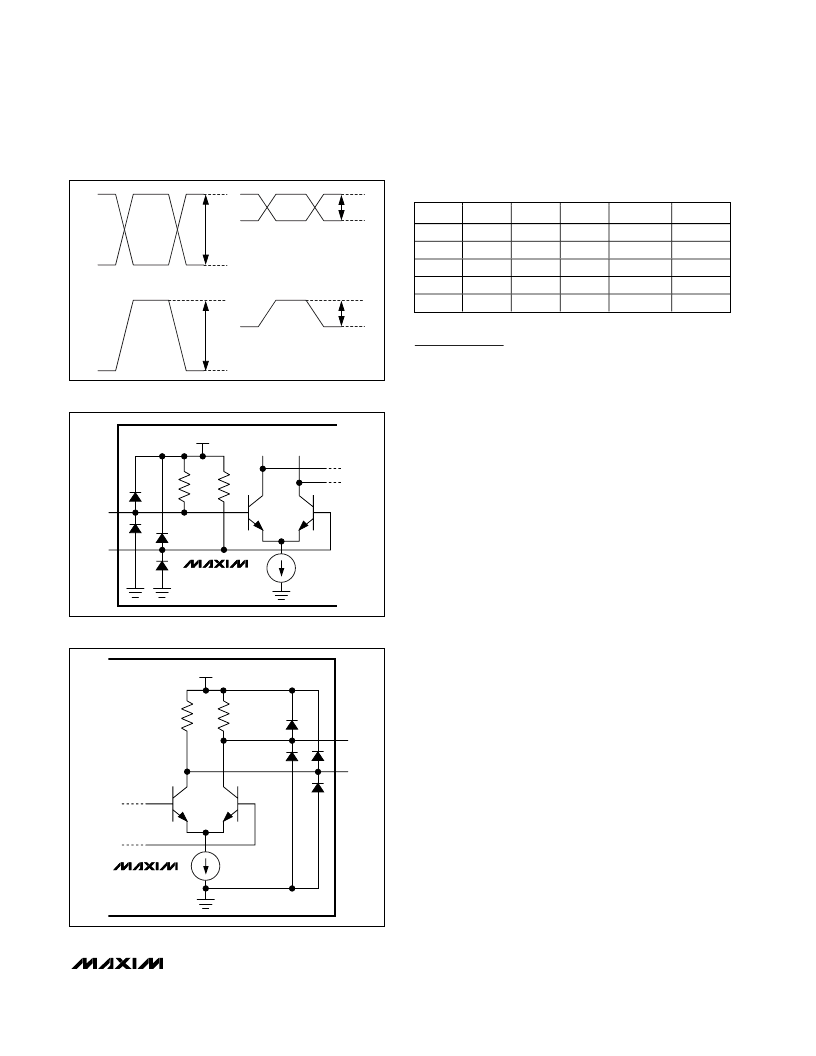
M
12.5Gbps CML 2
×
2 Crosspoint Switch
_______________________________________________________________________________________
5
V-
V+
(V+) - (V-)
1200mV
MAX
600mV
MAX
75mV
MIN
150mV
MIN
Figure 2. Definition of Differential Voltage Swing
MAX3841
50
50
VCC_IN
IN_+
IN_-
MAX3841
50
50
VCC_OUT
OUT_+
OUT_-
Figure 3. Equivalent CML Input Circuit
Figure 4. Equivalent CML Output Circuit
Table 1. Output Controls
ENO1
0
0
0
0
1
ENO2
0
0
0
0
1
SEL1
0
0
1
1
X
SEL2
0
1
0
1
X
OUT1
IN2
IN2
IN1
IN1
Disabled
OUT2
IN1
IN2
IN1
IN2
Disabled
相關(guān)PDF資料 |
PDF描述 |
|---|---|
| MAX385EJE | Precision, Low-Voltage Analog Switches |
| MAX381EJE | Precision, Low-Voltage Analog Switches |
| MAX381 | Precision, Low-Voltage Analog Switches |
| MAX381MJE | Precision, Low-Voltage Analog Switches |
| MAX383CPE | Precision, Low-Voltage Analog Switches |
相關(guān)代理商/技術(shù)參數(shù) |
參數(shù)描述 |
|---|---|
| MAX3841ETG+ | 功能描述:模擬和數(shù)字交叉點(diǎn) IC 12.5Gbps CML 2x2 Crosspoint Switch RoHS:否 制造商:Micrel 配置:2 x 2 封裝 / 箱體:MLF-16 數(shù)據(jù)速率:10.7 Gbps 輸入電平:CML, LVDS, LVPECL 輸出電平:CML 電源電壓-最大:3.6 V 電源電壓-最小:2.375 V 最大工作溫度:+ 85 C 最小工作溫度:- 40 C 產(chǎn)品:Digital Crosspoint 封裝:Tube |
| MAX3841ETG+T | 功能描述:模擬和數(shù)字交叉點(diǎn) IC 12.5Gbps CML 2x2 Crosspoint Switch RoHS:否 制造商:Micrel 配置:2 x 2 封裝 / 箱體:MLF-16 數(shù)據(jù)速率:10.7 Gbps 輸入電平:CML, LVDS, LVPECL 輸出電平:CML 電源電壓-最大:3.6 V 電源電壓-最小:2.375 V 最大工作溫度:+ 85 C 最小工作溫度:- 40 C 產(chǎn)品:Digital Crosspoint 封裝:Tube |
| MAX3841ETG-T | 功能描述:模擬和數(shù)字交叉點(diǎn) IC 12.5Gbps CML 2x2 Crosspoint Switch RoHS:否 制造商:Micrel 配置:2 x 2 封裝 / 箱體:MLF-16 數(shù)據(jù)速率:10.7 Gbps 輸入電平:CML, LVDS, LVPECL 輸出電平:CML 電源電壓-最大:3.6 V 電源電壓-最小:2.375 V 最大工作溫度:+ 85 C 最小工作溫度:- 40 C 產(chǎn)品:Digital Crosspoint 封裝:Tube |
| MAX3841EVKIT | 功能描述:模擬和數(shù)字交叉點(diǎn) IC Evaluation Kit for the MAX3841 RoHS:否 制造商:Micrel 配置:2 x 2 封裝 / 箱體:MLF-16 數(shù)據(jù)速率:10.7 Gbps 輸入電平:CML, LVDS, LVPECL 輸出電平:CML 電源電壓-最大:3.6 V 電源電壓-最小:2.375 V 最大工作溫度:+ 85 C 最小工作溫度:- 40 C 產(chǎn)品:Digital Crosspoint 封裝:Tube |
| MAX3845EVKIT+ | 功能描述:視頻 IC Evaluation Kit for the MAX3845 and MAX4814E RoHS:否 制造商:Fairchild Semiconductor 工作電源電壓:5 V 電源電流:80 mA 最大工作溫度:+ 85 C 封裝 / 箱體:TSSOP-28 封裝:Reel |
發(fā)布緊急采購(gòu),3分鐘左右您將得到回復(fù)。