- 您現(xiàn)在的位置:買(mǎi)賣(mài)IC網(wǎng) > PDF目錄384663 > MAX3314 (Maxim Integrated Products, Inc.) 5V High-Speed RS-232 Transceivers with 0.1uF Capacitors PDF資料下載
參數(shù)資料
| 型號(hào): | MAX3314 |
| 廠商: | Maxim Integrated Products, Inc. |
| 元件分類(lèi): | RS-232 |
| 英文描述: | 5V High-Speed RS-232 Transceivers with 0.1uF Capacitors |
| 中文描述: | 5V的高速RS - 232收發(fā)器與0.1uF電容 |
| 文件頁(yè)數(shù): | 2/6頁(yè) |
| 文件大小: | 196K |
| 代理商: | MAX3314 |
M
460kbps, 1μA, RS-232-Compatible Transceiver
2
_______________________________________________________________________________________
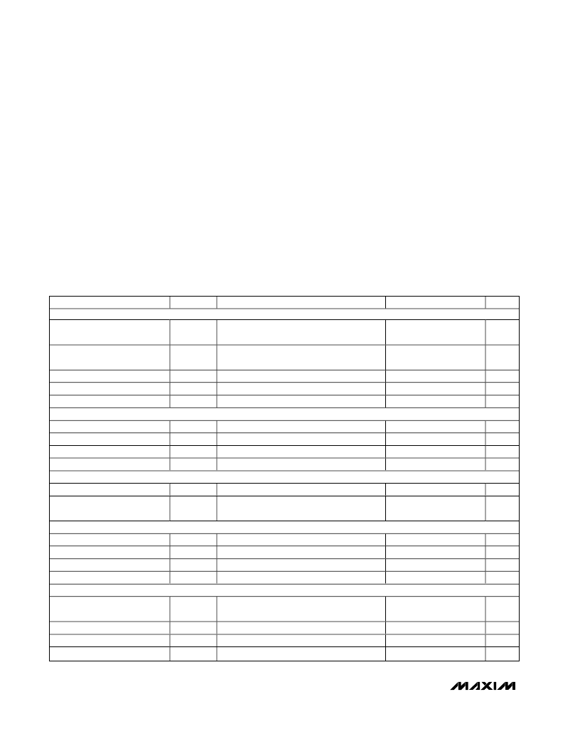
ABSOLUTE MAXIMUM RATINGS
V
CC
to GND..............................................................-0.3V to +6V
V- to GND.................................................................+0.3V to -6V
Input Voltages
TIN,
SHDN
to GND..............................................-0.3V to +6V
RIN to GND.....................................................................±25V
Output Voltages
TOUT to GND...............................................................±13.2V
ROUT.................................................…-0.3V to (V
CC
+ 0.3V)
Short-Circuit Duration
TOUT to GND........................................................Continuous
ELECTRICAL CHARACTERISTICS
(V
CC
= +5V, V- = -5V, T
A
= T
MIN
to T
MAX
, unless otherwise noted. Typical values are at T
A
= +25°C.)
PARAMETER
SYMBOL
DC CHARACTERISTICS
Positive Supply Operating
Range
Negative Supply Operating
Range
Positive Supply Current
SHDN
= V
CC
, no load
Negative Supply Current
SHDN
= V
CC
, no load
Shutdown Supply Current
SHDN
= GND
LOGIC INPUTS
(TIN,
SHDN
)
Input Logic Threshold Low
V
IL
Input Logic Threshold High
V
IH
Transmitter Input Hysteresis
Input Leakage Current
RECEIVER OUTPUT
Output Voltage Low
V
OL
I
OUT
= 1.6mA
Stresses beyond those listed under “Absolute Maximum Ratings” may cause permanent damage to the device. These are stress ratings only, and functional
operation of the device at these or any other conditions beyond those indicated in the operational sections of the specifications is not implied. Exposure to
absolute maximum rating conditions for extended periods may affect device reliability.
Note 1:
Not tested—guaranteed by design.
Continuous Power Dissipation
8-Pin SOT23 (derate 9.7mW/°C above +70°C)...........777mW
8-Pin μMAX (derate 4.1mW/°C above +70°C)............300mW
8-Pin SO (derate 5.88mW/°C above +70°C)...............471mW
Operating Temperature Ranges
MAX3314C_A.....................................................0°C to +70°C
MAX3314E_A..................................................-40°C to +85°C
Junction Temperature.....................................................+150°C
Storage Temperature Range............................-65°C to +150°C
Lead Temperature (soldering, 10s)................................+300°C
CONDITIONS
MIN
TYP
MAX
UNITS
V
CC
4.75
5
5.25
V
V-
-4.75
-5
-5.25
V
30
15
1
100
30
10
μ
A
μ
A
μ
A
0.8
V
V
V
μ
A
2.4
0.5
±
0.01
0.4
V
Output Voltage High
V
OH
I
OUT
= -1.0mA
V
CC
- 0.3
V
CC
- 0.1
V
RECEIVER INPUT
Input Threshold Low
Input Threshold High
Input Hysteresis
Input Resistance
TRANSMITTER OUTPUT
V
IL
V
IH
0.8
V
V
V
2.4
0.5
5
k
Output Voltage Swing
Transmitter output loaded with 3k
to
ground
V
CC
= V- = 0, transmitter output =
±
2V
V
OUT
=
±
12V, transmitter disabled
±
3.7
V
Output Resistance (Note 1)
Output Short-Circuit Current
Output Leakage Current
300
mA
μ
A
±
60
25
相關(guān)PDF資料 |
PDF描述 |
|---|---|
| MAX3314CEKA | Interface IC |
| MAX3314CEUA | Interface IC |
| MAX3314CKA | POWER CHASSIS MED 700W 6 SLOT |
| MAX3314EUA | 5V High-Speed RS-232 Transceivers with 0.1uF Capacitors |
| MAX3314EKA | 5V High-Speed RS-232 Transceivers with 0.1uF Capacitors |
相關(guān)代理商/技術(shù)參數(shù) |
參數(shù)描述 |
|---|---|
| MAX3314CKA | 制造商:Maxim Integrated Products 功能描述:- Cut Tape Product |
| MAX3314CKA+ | 制造商:Maxim Integrated Products 功能描述:LINE TRANSMITTER/RCVR 1TR 1TX 1RX 8PIN SOT-23 - Cut Tape Product |
| MAX3314CKA+T | 功能描述:RS-232接口集成電路 460kbps 1uA Transceiver RoHS:否 制造商:Exar 數(shù)據(jù)速率:52 Mbps 工作電源電壓:5 V 電源電流:300 mA 工作溫度范圍:- 40 C to + 85 C 安裝風(fēng)格:SMD/SMT 封裝 / 箱體:LQFP-100 封裝: |
| MAX3314CKA-T | 功能描述:RS-232接口集成電路 RoHS:否 制造商:Exar 數(shù)據(jù)速率:52 Mbps 工作電源電壓:5 V 電源電流:300 mA 工作溫度范圍:- 40 C to + 85 C 安裝風(fēng)格:SMD/SMT 封裝 / 箱體:LQFP-100 封裝: |
| MAX3314CSA | 功能描述:RS-232接口集成電路 RoHS:否 制造商:Exar 數(shù)據(jù)速率:52 Mbps 工作電源電壓:5 V 電源電流:300 mA 工作溫度范圍:- 40 C to + 85 C 安裝風(fēng)格:SMD/SMT 封裝 / 箱體:LQFP-100 封裝: |
發(fā)布緊急采購(gòu),3分鐘左右您將得到回復(fù)。