- 您現(xiàn)在的位置:買賣IC網(wǎng) > PDF目錄10636 > MAX3301EETJ+ (Maxim Integrated Products)IC USB TXRX OTG 32-TQFN-EP PDF資料下載
參數(shù)資料
| 型號: | MAX3301EETJ+ |
| 廠商: | Maxim Integrated Products |
| 文件頁數(shù): | 13/38頁 |
| 文件大小: | 0K |
| 描述: | IC USB TXRX OTG 32-TQFN-EP |
| 產(chǎn)品培訓(xùn)模塊: | Lead (SnPb) Finish for COTS Obsolescence Mitigation Program |
| 標(biāo)準(zhǔn)包裝: | 60 |
| 類型: | 收發(fā)器 |
| 規(guī)程: | USB 2.0 |
| 電源電壓: | 3 V ~ 4.5 V |
| 安裝類型: | 表面貼裝 |
| 封裝/外殼: | 32-WFQFN 裸露焊盤 |
| 供應(yīng)商設(shè)備封裝: | 32-TQFN-EP(5x5) |
| 包裝: | 管件 |
| 產(chǎn)品目錄頁面: | 1406 (CN2011-ZH PDF) |
第1頁第2頁第3頁第4頁第5頁第6頁第7頁第8頁第9頁第10頁第11頁第12頁當(dāng)前第13頁第14頁第15頁第16頁第17頁第18頁第19頁第20頁第21頁第22頁第23頁第24頁第25頁第26頁第27頁第28頁第29頁第30頁第31頁第32頁第33頁第34頁第35頁第36頁第37頁第38頁
MAX3301E/MAX3302E
USB On-the-Go Transceivers and Charge Pumps
20
______________________________________________________________________________________
of the MAX3301E/MAX3302E’s slave address, followed
by a 1 (R/
W bit). The master then reads one or more
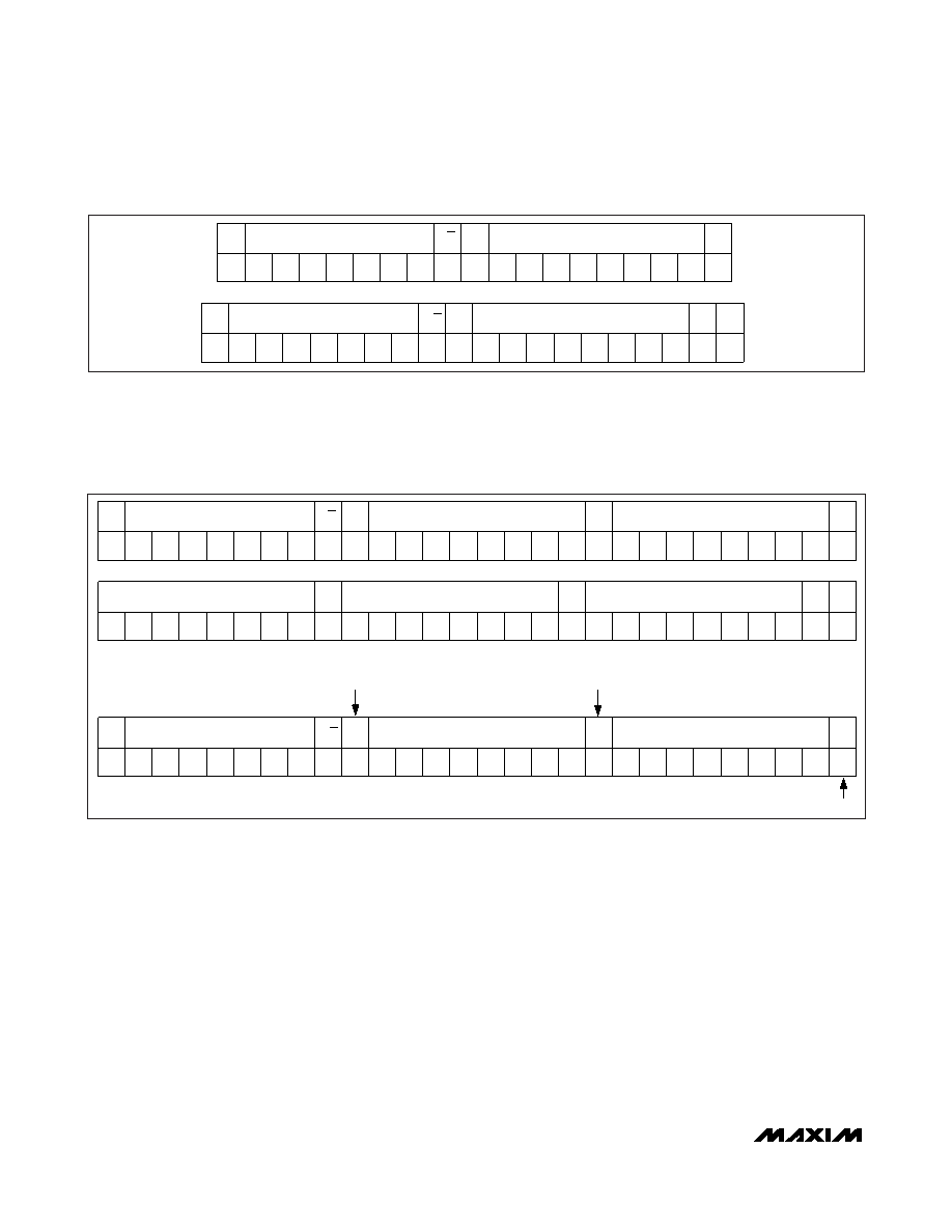
bytes of data. Figure 19 shows the typical read byte
format.
Burst-Mode Write Byte Format
The MAX3301E/MAX3302E allow a master device to
write to sequential registers without repeatedly sending
the slave address and register address each time. The
master first sends the slave address, followed by a 0 to
write data to the MAX3301E/MAX3302E. The
MAX3301E/MAX3302E send an acknowledge bit back
to the master. The master sends the 8-bit register
address and the MAX3301E/MAX3302E return an
acknowledge bit. The master writes a data byte to the
selected register and receives an acknowledge bit if a
supported register address has been chosen. The reg-
ister address increments and is ready for the master to
send the next data byte. The MAX3301E/MAX3302E
send an acknowledge bit after each data byte. If an
unsupported register is selected, the MAX3301E/
MAX3302E send a NACK to the master and the register
index does not increment (see Figure 20).
S
SLAVE ADDRESS
(7 BITS)
A6
A5
A4
A3
A2
A1
A0
0
A
REGISTER ADDRESS (K)
(8 BITS)
MSB
LSB
AA
MSB
LSB
DATA (K)
(8 BITS)
DATA (K+1)
(8 BITS)
A
DATA (K+2)
(8 BITS)
MSB
LSB
AA
MSB
LSB
DATA (K+N)
(8 BITS)
MSB
LSB
P
S
SLAVE ADDRESS
(7 BITS)
A6
A5
A4
A3
A2
A1
A0
0
A
UNSUPPORTED REGISTER ADDRESS (K)
(8 BITS)
MSB
LSB
ANA
MSB
LSB
DATA (K)
(8 BITS)
MAX3301E/MAX3302E RECOGNIZES
ITS ADDRESS
MAX3301E/MAX3302E SENDS
AN ACK
MAX3301E/MAX3302E RECOGNIZES A WRITE TO AN
UNSUPPORTED LOCATION, THEN SENDS A NACK
R/W
Figure 20. Burst-Mode Write Byte Format
S
SLAVE ADDRESS
(7 BITS)
A6
A5
A4
A3
A2
A1
A0
0
A
REGISTER ADDRESS
(8 BITS)
MSB
LSB
A
RS
SLAVE ADDRESS
(7 BITS)
A6
A5
A4
A3
A2
A1
A0
1
0
A
DATA
(8 BITS)
MSB
LSB
NA
P
R/W
Figure 19. Read Byte Format
R/
W: Read/write (R/W = 1: read; R/W = 0: write)
S: Start condition
RS: Repeated start condition
P: Stop condition
A: Acknowledge bit from the slave
NA: Not-acknowledged bit from the master
Blank: Master transmission
相關(guān)PDF資料 |
PDF描述 |
|---|---|
| VE-BWV-MX-F4 | CONVERTER MOD DC/DC 5.8V 75W |
| VE-BWV-MX-F3 | CONVERTER MOD DC/DC 5.8V 75W |
| VE-BWV-MX-F2 | CONVERTER MOD DC/DC 5.8V 75W |
| VE-B1F-IV-F2 | CONVERTER MOD DC/DC 72V 150W |
| VE-BWV-MX-F1 | CONVERTER MOD DC/DC 5.8V 75W |
相關(guān)代理商/技術(shù)參數(shù) |
參數(shù)描述 |
|---|---|
| MAX3301EETJ+ | 功能描述:USB 接口集成電路 USB On-the-Go Tcvr & Charge Pump RoHS:否 制造商:Cypress Semiconductor 產(chǎn)品:USB 2.0 數(shù)據(jù)速率: 接口類型:SPI 工作電源電壓:3.15 V to 3.45 V 工作電源電流: 最大工作溫度:+ 85 C 安裝風(fēng)格:SMD/SMT 封裝 / 箱體:WLCSP-20 |
| MAX3301EETJ+GH7 | 功能描述:USB 接口集成電路 USB On-the-Go Transceiver and Charge Pump RoHS:否 制造商:Cypress Semiconductor 產(chǎn)品:USB 2.0 數(shù)據(jù)速率: 接口類型:SPI 工作電源電壓:3.15 V to 3.45 V 工作電源電流: 最大工作溫度:+ 85 C 安裝風(fēng)格:SMD/SMT 封裝 / 箱體:WLCSP-20 |
| MAX3301EETJ+T | 功能描述:USB 接口集成電路 USB On-the-Go Tcvr & Charge Pump RoHS:否 制造商:Cypress Semiconductor 產(chǎn)品:USB 2.0 數(shù)據(jù)速率: 接口類型:SPI 工作電源電壓:3.15 V to 3.45 V 工作電源電流: 最大工作溫度:+ 85 C 安裝風(fēng)格:SMD/SMT 封裝 / 箱體:WLCSP-20 |
| MAX3301EETJ+TGH7 | 功能描述:USB 接口集成電路 USB On-the-Go Transceivers and Charge Pumps RoHS:否 制造商:Cypress Semiconductor 產(chǎn)品:USB 2.0 數(shù)據(jù)速率: 接口類型:SPI 工作電源電壓:3.15 V to 3.45 V 工作電源電流: 最大工作溫度:+ 85 C 安裝風(fēng)格:SMD/SMT 封裝 / 箱體:WLCSP-20 |
| MAX3301EETJ-T | 功能描述:USB 接口集成電路 RoHS:否 制造商:Cypress Semiconductor 產(chǎn)品:USB 2.0 數(shù)據(jù)速率: 接口類型:SPI 工作電源電壓:3.15 V to 3.45 V 工作電源電流: 最大工作溫度:+ 85 C 安裝風(fēng)格:SMD/SMT 封裝 / 箱體:WLCSP-20 |
發(fā)布緊急采購,3分鐘左右您將得到回復(fù)。