- 您現(xiàn)在的位置:買賣IC網(wǎng) > PDF目錄383362 > MAX3266CSA (MAXIM INTEGRATED PRODUCTS INC) 32-Bit Digital Signal Controller with Flash 100-LQFP -40 to 125 PDF資料下載
參數(shù)資料
| 型號: | MAX3266CSA |
| 廠商: | MAXIM INTEGRATED PRODUCTS INC |
| 元件分類: | 通信及網(wǎng)絡(luò) |
| 英文描述: | 32-Bit Digital Signal Controller with Flash 100-LQFP -40 to 125 |
| 中文描述: | SPECIALTY TELECOM CIRCUIT, PDSO8 |
| 封裝: | 0.150 INCH, SOIC-8 |
| 文件頁數(shù): | 6/8頁 |
| 文件大小: | 152K |
| 代理商: | MAX3266CSA |

M
1.25Gbps/2.5Gbps, 3V to 5.5V, Low-Noise
Transimpedanc e Preamplifiers for LANs
6
_______________________________________________________________________________________
Output Filter
The MAX3266 includes a 1-pole lowpass filter which
limits the circuit bandwidth and improves noise perform-
ance.
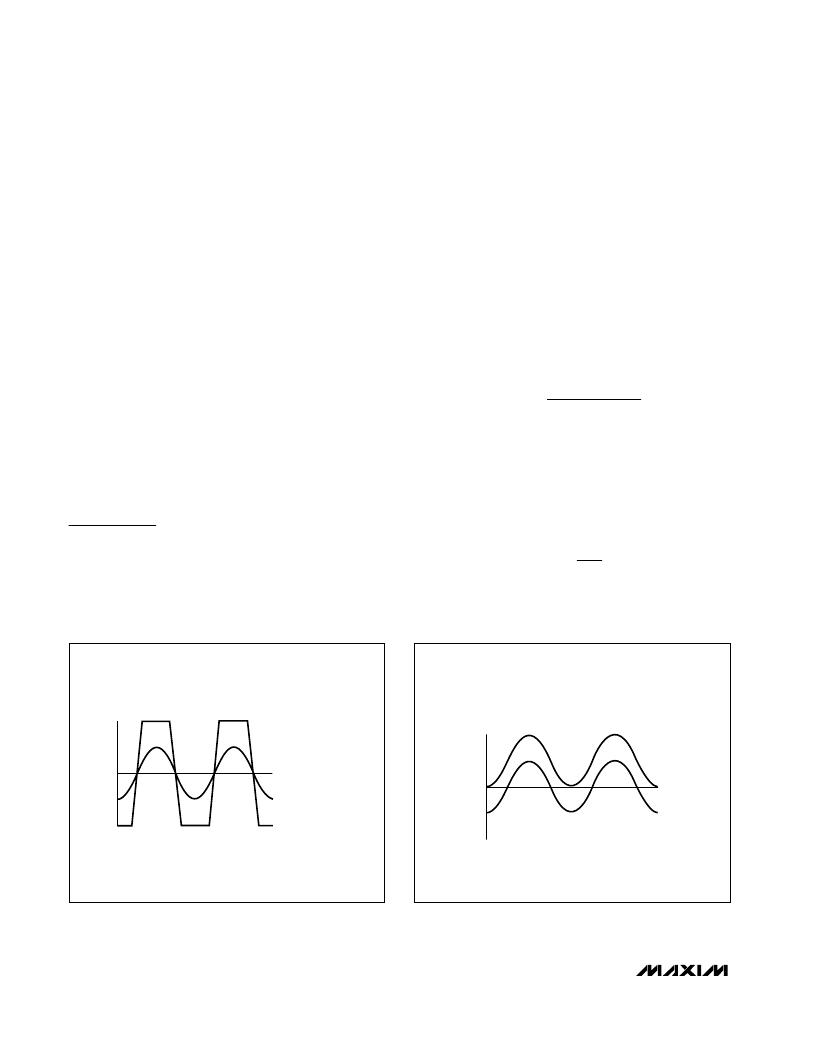
DC Canc ellation Circ uit
The DC cancellation circuit uses low-frequency feed-
back to remove the DC component of the input signal
(Figure 4). This feature centers the input signal within
the transimpedance amplifier’s linear range, thereby
reducing pulse-width distortion on large input signals.
The DC cancellation circuit is internally compensated
and therefore does not require external capacitors. This
circuit minimizes pulse-width distortion for data
sequences that exhibit a 50% duty cycle. A duty cycle
significantly different from 50% will cause the MAX3266
to generate pulse-width distortion.
DC cancellation current is drawn from the input and
creates noise. For low-level signals with little or no DC
component, this is not a problem. Amplifier noise will
increase for signals with significant DC component (see
Typical Operating Characteristics).
Applic ations Information
Optic al Power Relations
Many of the MAX3266 specifications relate to the input
signal amplitude. When working with fiber optic
receivers, the input is usually expressed in terms of aver-
age optical power and extinction ratio. Figure 5 shows
relations that are helpful for converting optical power to
input signal when designing with the MAX3266.
Optical power relations are shown in Table 1; the defini-
tions are true if the average duty cycle of the input data
is 50%.
Optic al S ensitivity Calc ulation
The input-referred RMS noise current (I
N
) of the
MAX3266 generally determines the receiver sensitivity.
To obtain a system bit error rate (BER) of 1E-12, the
signal-to-noise ratio must always exceed 14.1. The
input sensitivity, expressed in average power, can be
estimated as:
2
ρ
Where
ρ
is the photodiode responsivity in A/W.
Input Optic al Overload
The overload is the largest input that the MAX3266
accepts while meeting specifications. The optical over-
load can be estimated in terms of average power with
the following equation:
Overload
mA
1
2
dBm
log
=
10
1000
ρ
Sensitivity
I
(
r
r
dBm
N
e
e
=
+
)
(
)
10
14.
1
1
1000
log
AMPLITUDE
OUTPUT (LARGE SIGNALS)
TIME
OUTPUT (SMALL SIGNALS)
Figure 3. MAX3266 Limited Output
Figure 4 . DC Cancellation Effect On Input
AMPLITUDE
INPUT FROM PHOTODIODE
TIME
INPUT (AFTER DC CANCELLATION)
相關(guān)PDF資料 |
PDF描述 |
|---|---|
| MAX3267CSA | 1.25Gbps/2.5Gbps, 3V to 5.5V, Low-Noise Transimpedance Preamplifiers for LANs |
| MAX3271 | +3.3V, 2.5Gbps Low-Power Transimpedance Amplifier |
| MAX3271D | +3.3V, 2.5Gbps Low-Power Transimpedance Amplifier |
| MAX3271E | +3.3V, 2.5Gbps Low-Power Transimpedance Amplifier |
| MAX3271W | +3.3V, 2.5Gbps Low-Power Transimpedance Amplifier |
相關(guān)代理商/技術(shù)參數(shù) |
參數(shù)描述 |
|---|---|
| MAX3266CSA+ | 功能描述:特殊用途放大器 RoHS:否 制造商:Texas Instruments 通道數(shù)量:Single 共模抑制比(最小值): 輸入補償電壓: 工作電源電壓:3 V to 5.5 V 電源電流:5 mA 最大功率耗散: 最大工作溫度:+ 70 C 最小工作溫度:- 40 C 安裝風(fēng)格:SMD/SMT 封裝 / 箱體:QFN-20 封裝:Reel |
| MAX3266CSA+T | 功能描述:特殊用途放大器 RoHS:否 制造商:Texas Instruments 通道數(shù)量:Single 共模抑制比(最小值): 輸入補償電壓: 工作電源電壓:3 V to 5.5 V 電源電流:5 mA 最大功率耗散: 最大工作溫度:+ 70 C 最小工作溫度:- 40 C 安裝風(fēng)格:SMD/SMT 封裝 / 箱體:QFN-20 封裝:Reel |
| MAX3266CSA-T | 功能描述:特殊用途放大器 RoHS:否 制造商:Texas Instruments 通道數(shù)量:Single 共模抑制比(最小值): 輸入補償電壓: 工作電源電壓:3 V to 5.5 V 電源電流:5 mA 最大功率耗散: 最大工作溫度:+ 70 C 最小工作溫度:- 40 C 安裝風(fēng)格:SMD/SMT 封裝 / 箱體:QFN-20 封裝:Reel |
| MAX3266EVKIT | 制造商:Maxim Integrated Products 功能描述:1.25GBPS 2.5GBPS, 3V TO 5.5V, LOW NOISE TRANS - Bulk |
| MAX3267C/D | 功能描述:特殊用途放大器 RoHS:否 制造商:Texas Instruments 通道數(shù)量:Single 共模抑制比(最小值): 輸入補償電壓: 工作電源電壓:3 V to 5.5 V 電源電流:5 mA 最大功率耗散: 最大工作溫度:+ 70 C 最小工作溫度:- 40 C 安裝風(fēng)格:SMD/SMT 封裝 / 箱體:QFN-20 封裝:Reel |
發(fā)布緊急采購,3分鐘左右您將得到回復(fù)。